- 您現(xiàn)在的位置:買(mǎi)賣(mài)IC網(wǎng) > PDF目錄10003 > IDT723616L15PF (IDT, Integrated Device Technology Inc)IC FIFO TRPL BUS 64X36X2 128QFP PDF資料下載
參數(shù)資料
| 型號(hào): | IDT723616L15PF |
| 廠商: | IDT, Integrated Device Technology Inc |
| 文件頁(yè)數(shù): | 2/26頁(yè) |
| 文件大?。?/td> | 0K |
| 描述: | IC FIFO TRPL BUS 64X36X2 128QFP |
| 標(biāo)準(zhǔn)包裝: | 72 |
| 系列: | 7200 |
| 功能: | 同步 |
| 存儲(chǔ)容量: | 4.6K(64 x 36 x2) |
| 數(shù)據(jù)速率: | 67MHz |
| 訪問(wèn)時(shí)間: | 15ns |
| 電源電壓: | 4.5 V ~ 5.5 V |
| 工作溫度: | 0°C ~ 70°C |
| 安裝類(lèi)型: | 表面貼裝 |
| 封裝/外殼: | 128-LQFP |
| 供應(yīng)商設(shè)備封裝: | 128-TQFP(14x20) |
| 包裝: | 托盤(pán) |
| 其它名稱(chēng): | 723616L15PF |
第1頁(yè)當(dāng)前第2頁(yè)第3頁(yè)第4頁(yè)第5頁(yè)第6頁(yè)第7頁(yè)第8頁(yè)第9頁(yè)第10頁(yè)第11頁(yè)第12頁(yè)第13頁(yè)第14頁(yè)第15頁(yè)第16頁(yè)第17頁(yè)第18頁(yè)第19頁(yè)第20頁(yè)第21頁(yè)第22頁(yè)第23頁(yè)第24頁(yè)第25頁(yè)第26頁(yè)
10
COMMERCIALANDINDUSTRIAL
TEMPERATURERANGES
IDT723616 CMOS TRIPLE BUS SyncFIFO
WITH
BUS-MATCHING AND BYTE SWAPPING 64 x 36 x 2
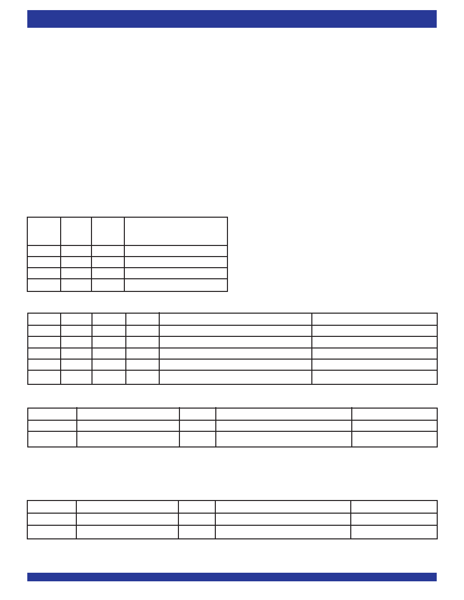
TABLE 4 — PORT-C ENABLE FUNCTION TABLE
NOTE:
1. At no time during the operation of the FIFO is it permissible to apply a LOW logic level simultaneously to both SIZ0 and SIZ1, nor is it permissible to apply a HIGH logic level
simultaneously to both these inputs. These state combinations are reserved.
WENC
SIZ1, SIZ0
CLKC
C0-C17 Inputs
Port Functions
L
X
In High-Impedance State
None
H
One or the other LOW(1)
↑
In High-Impedance State
FIFO2 write
SIGNALDESCRIPTIONS
RESET
The IDT723616 is reset by taking the reset (
RST) input LOW for at least
four Port A clock (CLKA), four Port B clock (CLKB) and four Port C clock
(CLKC) LOW-to-HIGH transitions. The reset input can switch asynchro-
nously to the clocks. A device reset initializes the internal read and write
pointers of each FIFO and forces the full flags (
FFA, FFC) LOW, the empty
flags (
EFA, EFB) LOW, the Almost-Empty flags (AEA, AEB) LOW and the
Almost-Full flags (
AFA, AFC) HIGH. After a reset, FFA is set HIGH after
two LOW-to-HIGH transitions of CLKA and FFC is set HIGH after two
LOW-to-HIGH transitions of CLKC. The device must be reset after power
up before data is written to its memory.
A LOW-to-HIGH transition on the
RST input loads the Almost-Full and
Almost-Empty Offset register (X) with the values selected by the flag-
select (FS0, FS1) inputs. The values that can be loaded into the registers
are shown in Table 1.
TABLE 2 — PORT-A ENABLE FUNCTION TABLE
FIFO WRITE/READ OPERATION
The state of Port A data A0-A35 outputs is controlled by the Port A chip
select (
CSA)andthePortAwrite/readselect(W/RA).TheA0-A35outputsare
in the high-impedance state when either
CSA or W/RA is HIGH. The A0-A35
outputs are active when both CSA and W/
RA are LOW. Data is loaded into
FIFO1 from the A0-A35 inputs on a LOW-to-HIGH transition of CLKA when
CSA is LOW, W/RA is HIGH, ENA is HIGH, and FFA is HIGH. Data is read
fromFIFO2totheA0-A35outputsbyaLOW-to-HIGHtransitionofCLKAwhen
CSA is LOW, W/
RA is LOW, ENA is HIGH, and EFA is HIGH (see Table 2).
The state of the Port B data (B0-B17) outputs is controlled by Port B read
select (RENB). The B0-B17 outputs are in the high-impedance state when
REN is LOW. The B0-B17 outputs are active when REN IS HIGH. Data is
read from FIFO1 to the B0-B17 outputs by a LOW-to-HIGH transition of
CLKB when RENB is HIGH,
EFB is HIGH, and either SIZ0 or SIZ1 is LOW
(see Table 3).
Data is loaded into FIFO2 from the C0-C17 inputs on a LOW-to-HIGH
transition of CLKC when WENC is HIGH,
FFC is HIGH, and either SIZ0 or
SIZ1 is LOW (see Table 4).
ThesetupandholdtimeconstraintstothePortClocksforthePortAchipselect
(CSA) and write/read selects (W/
RA, RENB, WENC) are only for enabling
write and read operations and are not related to high-impedance control of the
data outputs. If a port enable is LOW during a clock cycle, the Port Chip select
(for Port A) and write/read select (for all ports) can change states during the
setup and hold time window of the cycle.
TABLE 1 — FLAG PROGRAMMING
TABLE 3 — PORT-B ENABLE FUNCTION TABLE
NOTE:
1. At no time during the operation of the FIFO is it permissible to apply a LOW logic level simultaneously to both SIZ0 and SIZ1, nor is it permissible to apply a HIGH logic level
simultaneously to both these inputs. These state combinations are reserved.
ALMOST-FULL AND
FS1
FS0
RST
ALMOST-EMPTY FLAG
OFFSET REGISTER (X)
HH
↑
16
HL
↑
12
LH
↑
8
LL
↑
4
CSA
W/
RA
ENA
CLKA
A0-A35 Outputs
Port Functions
H
X
In High-Impedance State
None
L
H
L
X
In High-Impedance State
None
LH
H
↑
In High-Impedance State
FIFO1 Write
L
X
Active, FIFO2 Output Register
None
LL
H
↑
Active, FIFO2 Output Register
FIFO2 Read
RENB
SIZ1, SIZ0
CLKB
B0-B17 Outputs
Port Functions
L
X
In High-Impedance State
None
H
One or the other LOW(1)
↑
Active, FIFO1 Output Register
FIFO1 read
相關(guān)PDF資料 |
PDF描述 |
|---|---|
| IDT72V3614L15PF | IC FIFO 64X36X2 15NS 120QFP |
| ADV7511KSTZ-P | IC XMITTER HDMI 12BIT 100LQFP |
| VI-26P-IW-F4 | CONVERTER MOD DC/DC 13.8V 100W |
| MS27473T14F18PD | CONN PLUG 18POS STRAIGHT W/PINS |
| MS27467T15F97PB | CONN PLUG 12POS STRAIGHT W/PINS |
相關(guān)代理商/技術(shù)參數(shù) |
參數(shù)描述 |
|---|---|
| IDT723616L15PF8 | 功能描述:IC FIFO TRPL BUS 64X36X2 128QFP RoHS:否 類(lèi)別:集成電路 (IC) >> 邏輯 - FIFO 系列:7200 標(biāo)準(zhǔn)包裝:90 系列:7200 功能:同步 存儲(chǔ)容量:288K(16K x 18) 數(shù)據(jù)速率:100MHz 訪問(wèn)時(shí)間:10ns 電源電壓:4.5 V ~ 5.5 V 工作溫度:0°C ~ 70°C 安裝類(lèi)型:表面貼裝 封裝/外殼:64-LQFP 供應(yīng)商設(shè)備封裝:64-TQFP(14x14) 包裝:托盤(pán) 其它名稱(chēng):72271LA10PF |
| IDT723616L15PFG | 功能描述:IC FIFO 64X36X2 15NS 128TQFP RoHS:是 類(lèi)別:集成電路 (IC) >> 邏輯 - FIFO 系列:7200 標(biāo)準(zhǔn)包裝:90 系列:7200 功能:同步 存儲(chǔ)容量:288K(16K x 18) 數(shù)據(jù)速率:100MHz 訪問(wèn)時(shí)間:10ns 電源電壓:4.5 V ~ 5.5 V 工作溫度:0°C ~ 70°C 安裝類(lèi)型:表面貼裝 封裝/外殼:64-LQFP 供應(yīng)商設(shè)備封裝:64-TQFP(14x14) 包裝:托盤(pán) 其它名稱(chēng):72271LA10PF |
| IDT723616L15PFG8 | 制造商:Integrated Device Technology Inc 功能描述:IC FIFO TRPL BUS 64X36X2 128QFP |
| IDT723616L20PF | 功能描述:IC FIFO TRPL BUS 64X36X2 128QFP RoHS:否 類(lèi)別:集成電路 (IC) >> 邏輯 - FIFO 系列:7200 標(biāo)準(zhǔn)包裝:90 系列:7200 功能:同步 存儲(chǔ)容量:288K(16K x 18) 數(shù)據(jù)速率:100MHz 訪問(wèn)時(shí)間:10ns 電源電壓:4.5 V ~ 5.5 V 工作溫度:0°C ~ 70°C 安裝類(lèi)型:表面貼裝 封裝/外殼:64-LQFP 供應(yīng)商設(shè)備封裝:64-TQFP(14x14) 包裝:托盤(pán) 其它名稱(chēng):72271LA10PF |
| IDT723616L20PF8 | 功能描述:IC FIFO TRPL BUS 64X36X2 128QFP RoHS:否 類(lèi)別:集成電路 (IC) >> 邏輯 - FIFO 系列:7200 標(biāo)準(zhǔn)包裝:90 系列:7200 功能:同步 存儲(chǔ)容量:288K(16K x 18) 數(shù)據(jù)速率:100MHz 訪問(wèn)時(shí)間:10ns 電源電壓:4.5 V ~ 5.5 V 工作溫度:0°C ~ 70°C 安裝類(lèi)型:表面貼裝 封裝/外殼:64-LQFP 供應(yīng)商設(shè)備封裝:64-TQFP(14x14) 包裝:托盤(pán) 其它名稱(chēng):72271LA10PF |
發(fā)布緊急采購(gòu),3分鐘左右您將得到回復(fù)。