- 您現(xiàn)在的位置:買賣IC網(wǎng) > PDF目錄10052 > IDT72125L50SO8 (IDT, Integrated Device Technology Inc)IC FIFO 1KX16 PAR-SER 28SOIC PDF資料下載
參數(shù)資料
| 型號: | IDT72125L50SO8 |
| 廠商: | IDT, Integrated Device Technology Inc |
| 文件頁數(shù): | 6/10頁 |
| 文件大?。?/td> | 0K |
| 描述: | IC FIFO 1KX16 PAR-SER 28SOIC |
| 標準包裝: | 1,000 |
| 系列: | 7200 |
| 功能: | 異步 |
| 存儲容量: | 16K (1K x 16) |
| 訪問時間: | 50ns |
| 電源電壓: | 4.5 V ~ 5.5 V |
| 工作溫度: | -40°C ~ 85°C |
| 安裝類型: | 表面貼裝 |
| 封裝/外殼: | 28-SOIC(0.345",8.77mm 寬) |
| 供應(yīng)商設(shè)備封裝: | 28-SOIC |
| 包裝: | 帶卷 (TR) |
| 其它名稱: | 72125L50SO8 |
5
INDUSTRIAL TEMPERATURE RANGE
IDT72105/72115/72125 PARALLEL-TO-SERIAL CMOS FIFO
256 x 16, 512 x 16, 1,024 x 16
AC TEST CONDITIONS
2665 tbl 07
NOTES:
1.
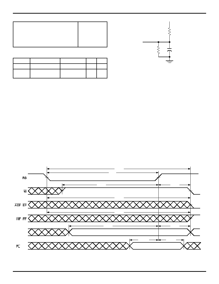
EF, FF, HF and AEF may change status during Reset, but flags will be valid at tRSC.
2.
SOCP should be in the steady LOW or HIGH during tRSS. The first LOW-HIGH (or HIGH-LOW) transition can begin after tRSR.
Figure 1. Reset
FUNCTIONAL DESCRIPTION
Parallel Data Input
The device must be reset before beginning operation so
that all flags are set to their initial state. In width or depth
expansion the First Load pin (
FL) must be programmed to
indicate the first device.
The data is written into the FIFO in parallel through the D0–
15
input data lines. A write cycle is initiated on the falling edge
of the Write (
W) signal provided the Full Flag (FF) is not
asserted. If the
W signal changes from HIGH-to-LOW and the
Full Flag (
FF) is already set, the write line is internally inhibited
internally from incrementing the write pointer and no write
operation occurs.
Data set-up and hold times must be met with respect to the
rising edge of Write. On the rising edge of
W, the write pointer
is incremented. Write operations can occur simultaneously or
asynchronously with read operations.
Serial Data Output
The serial data is output on the SO pin. The data is clocked
out on the rising edge of SOCP providing the Empty Flag (
EF)
is not asserted. If the Empty Flag is asserted then the next data
word is inhibited from moving to the output register and being
clocked out by SOCP.
The serial word is shifted out Least Significant Bit or Most
Significant Bit first, depending on the
FL/DIR level during
operation. A LOW on DIR will cause the Least Significant Bit
to be read out first. A HIGH on DIR will cause the Most
Significant Bit to be read out first.
CAPACITANCE (TA = +25
°C, f = 1.0MHz)
Symbol
Parameter(1)
Conditions
Max.
Unit
CIN
Input Capacitance
VIN = 0V
10
pF
COUT
Output
Capacitance
VOUT = 0V
12
pF
NOTE:
2665 tbl 08
1. Characterized values, not currently tested.
Input Pulse Levels
GND to 3.0V
Input Rise/Fall Times
5ns
Input Timing Reference Levels
1.5V
Output Reference Levels
1.5V
Output Load
See Figure A
2665 drw 03
1.1K
30pF
680
5V
TO
OUTPUT
PIN
*
or equivalent circuit
Figure A. Output Load
*Includes jig and scope capacitances.
tRSC
,
FLAG
STABLE
FLAG
STABLE
2665 drw 04
tRSC
tRSS
tRSR
tRSC
tRS
SOCP
tRSS
tRSR
NOTE 2
tFLS
tFLH
/DIR
相關(guān)PDF資料 |
PDF描述 |
|---|---|
| VI-2NL-IW-F4 | CONVERTER MOD DC/DC 28V 100W |
| LTC1347CSW#TR | IC TXRX RS232 5V LOW PWR 28SOIC |
| VI-24L-MY | CONVERTER MOD DC/DC 28V 50W |
| MS3100F20-29PW | CONN RCPT 17POS WALL MNT W/PINS |
| IDT72225LB10TF | IC FIFO 1024X18 SYNC 10NS 64TQFP |
相關(guān)代理商/技術(shù)參數(shù) |
參數(shù)描述 |
|---|---|
| IDT72125L50TP | 功能描述:IC FIFO 1KX16 PAR-SER 28DIP RoHS:否 類別:集成電路 (IC) >> 邏輯 - FIFO 系列:7200 標準包裝:90 系列:7200 功能:同步 存儲容量:288K(16K x 18) 數(shù)據(jù)速率:100MHz 訪問時間:10ns 電源電壓:4.5 V ~ 5.5 V 工作溫度:0°C ~ 70°C 安裝類型:表面貼裝 封裝/外殼:64-LQFP 供應(yīng)商設(shè)備封裝:64-TQFP(14x14) 包裝:托盤 其它名稱:72271LA10PF |
| IDT72131L50CB | 制造商:Integrated Device Technology Inc 功能描述: |
| IDT72131L50P | 制造商:Integrated Device Technology Inc 功能描述: |
| IDT72156 | 制造商:IDT 功能描述:72156 |
| IDT7216L25FB | 制造商:Integrated Device Technology Inc 功能描述:MULTIPLIER, 64 Pin, Ceramic, Quad CERPAK |
發(fā)布緊急采購,3分鐘左右您將得到回復(fù)。