- 您現(xiàn)在的位置:買賣IC網(wǎng) > PDF目錄360747 > ICS2595 User-Programmable Dual High-Performance Clock Generator PDF資料下載
參數(shù)資料
| 型號(hào): | ICS2595 |
| 英文描述: | User-Programmable Dual High-Performance Clock Generator |
| 中文描述: | 用戶可編程雙路高性能時(shí)鐘發(fā)生器 |
| 文件頁(yè)數(shù): | 3/12頁(yè) |
| 文件大?。?/td> | 272K |
| 代理商: | ICS2595 |
ICS2595
Digital Inputs
The
FS0-FS3
pins and the
STROBE
pin are used to select
the desired operating frequency of the
VCLK
output from
the 16 pre-programmed/user-programmed selections in
the
ICS2595
. These pins are also used to load new frequency
data into the registers.
The standard interface for the
ICS2595
matches the interface
of the industry standard ICS2494. That is, the FS0-FS3
inputs access the device internals transparently when the
STROBE pin is high.
The digital interface for the
ICS2595
(i.e. the
FS0-FS3
inputs) may be optionally configured for edge-triggered
or level-activated operation of the
STROBE
pin. Example
timing requirements for each of the four options are
shown in Figure 1.
The programming sequence has been designed in such a
way that
STROBE
pin need not be used (as in situations
where the device is connected to the frequency select port
of some VGA chips).
VCLK Output Frequency Selection
To change the
VCLK
output frequency, simply write the
appropriate data to the
ICS2595 FS
inputs. The synthesizer
will output the new frequency programmed into that location
after a brief delay (see time-out specifications).
Upon device power-up, the selected frequency will be the
frequency pre-programmed into address 0 until a device
write is performed.
MCLK Output Frequency Selection
The MS0-MS1 pins are used to directly select the desired
operating frequency of the MCLK output from the four
pre-programmed/user-programmed selections in the
ICS2595
. These inputs are not latched, nor are they involved
with memory programming operations.
Programming Mode Selection
In order to ensure that reliable programming under all
circumstances, we require that two "nibble" writes be
added to the beginning of the programming sequence that
was previously specified. The new sequence is shown in
Table 1. Note that the FS3 data is "0" for these first two
writes.
e
b
b
i
N
!
"
#
!
$
%
!
!
!
&
"
!
!
'
"
(
)
*
$
%
*
*
*
*
*
$
%
*
&
'
"
(
)
*
)
+
,
-
,
&
(
.
(
/
0
1
&
(
.
(
/
0
1
$
%
2
#
3
2
#
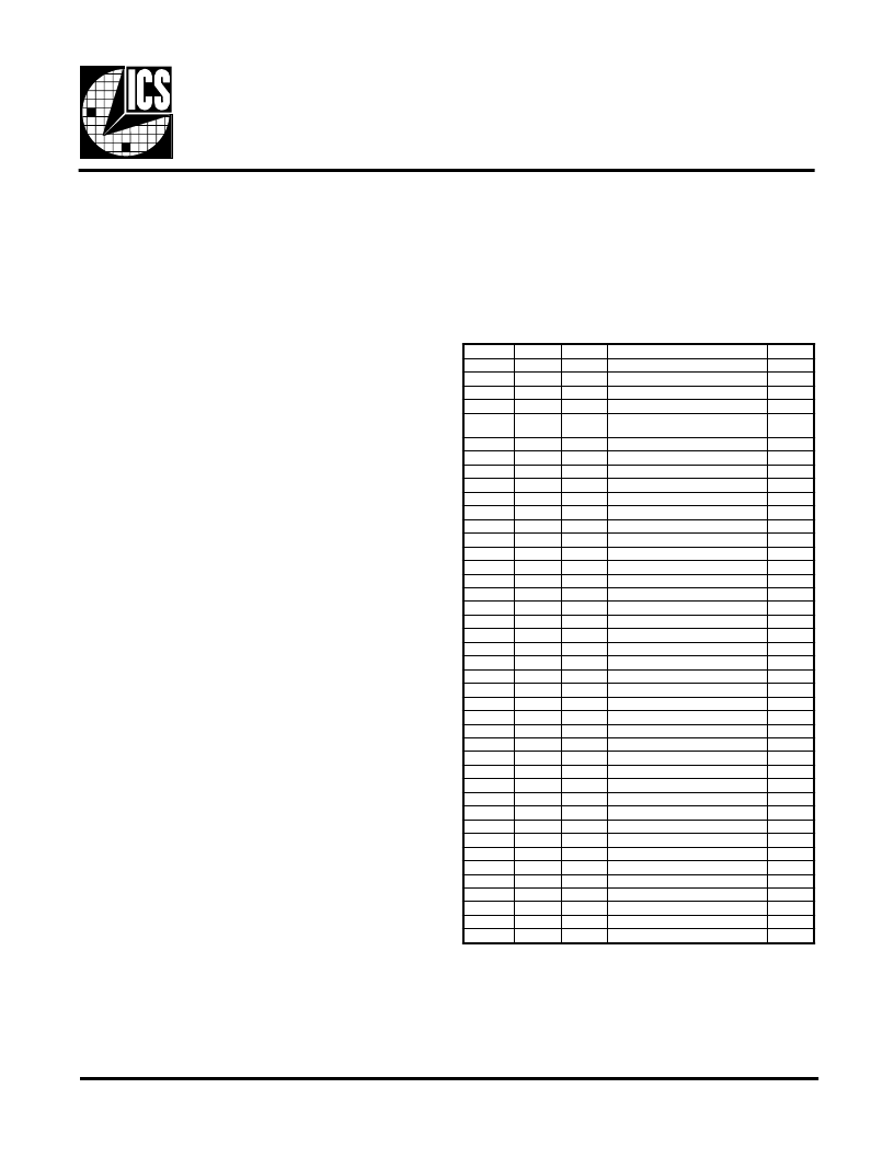
Table 1: Programming Sequence
Because the same pins are used for both VCLK frequency
selection and re-programming the device frequency table,
a specific procedure must be observed for selection between
these modes. Device programming is accomplished by
executing a "programming sequence". The latched FS2
input functions as a data input, and the latched FS3 input
functions as a data clock when this mode is activated. As
the latched FS3 data transitions from 0 to 1, the latched
FS2 data is shifted into the register. Note that it is the
相關(guān)PDF資料 |
PDF描述 |
|---|---|
| ICS2628M022 | Peripheral IC |
| ICS2628M034 | Peripheral IC |
| ICS2628N022 | Peripheral IC |
| ICS2628N034 | Peripheral IC |
| ICS2655M001 | Peripheral IC |
相關(guān)代理商/技術(shù)參數(shù) |
參數(shù)描述 |
|---|---|
| ICS2595M-S02 | 制造商:未知廠家 制造商全稱:未知廠家 功能描述:Video/Graphics Clock Generator |
| ICS2595M-S04 | 制造商:未知廠家 制造商全稱:未知廠家 功能描述:Video/Graphics Clock Generator |
| ICS2595N-S02 | 制造商:未知廠家 制造商全稱:未知廠家 功能描述:Video/Graphics Clock Generator |
| ICS2595N-S04 | 制造商:未知廠家 制造商全稱:未知廠家 功能描述:Video/Graphics Clock Generator |
| ICS2628M022 | 制造商:未知廠家 制造商全稱:未知廠家 功能描述:Peripheral IC |
發(fā)布緊急采購(gòu),3分鐘左右您將得到回復(fù)。