- 您現(xiàn)在的位置:買賣IC網(wǎng) > PDF目錄384476 > I5216SI (WINBOND ELECTRONICS CORP) 8 TO 16 MINUTE VOICE RECORD/PLAYBACK SYSTEM WITH INTEGRATED CODEC PDF資料下載
參數(shù)資料
| 型號: | I5216SI |
| 廠商: | WINBOND ELECTRONICS CORP |
| 元件分類: | 音頻合成 |
| 英文描述: | 8 TO 16 MINUTE VOICE RECORD/PLAYBACK SYSTEM WITH INTEGRATED CODEC |
| 中文描述: | 960 SEC, SPEECH SYNTHESIZER WITH RCDG, PDSO28 |
| 封裝: | 0.300 INCH, PLASTIC, SOIC-28 |
| 文件頁數(shù): | 5/83頁 |
| 文件大?。?/td> | 758K |
| 代理商: | I5216SI |
第1頁第2頁第3頁第4頁當(dāng)前第5頁第6頁第7頁第8頁第9頁第10頁第11頁第12頁第13頁第14頁第15頁第16頁第17頁第18頁第19頁第20頁第21頁第22頁第23頁第24頁第25頁第26頁第27頁第28頁第29頁第30頁第31頁第32頁第33頁第34頁第35頁第36頁第37頁第38頁第39頁第40頁第41頁第42頁第43頁第44頁第45頁第46頁第47頁第48頁第49頁第50頁第51頁第52頁第53頁第54頁第55頁第56頁第57頁第58頁第59頁第60頁第61頁第62頁第63頁第64頁第65頁第66頁第67頁第68頁第69頁第70頁第71頁第72頁第73頁第74頁第75頁第76頁第77頁第78頁第79頁第80頁第81頁第82頁第83頁
I5216 SERIES
Advanced Information
PRELIMINARY
Publication Release Date: November 30, 2001
-5
Revision A1
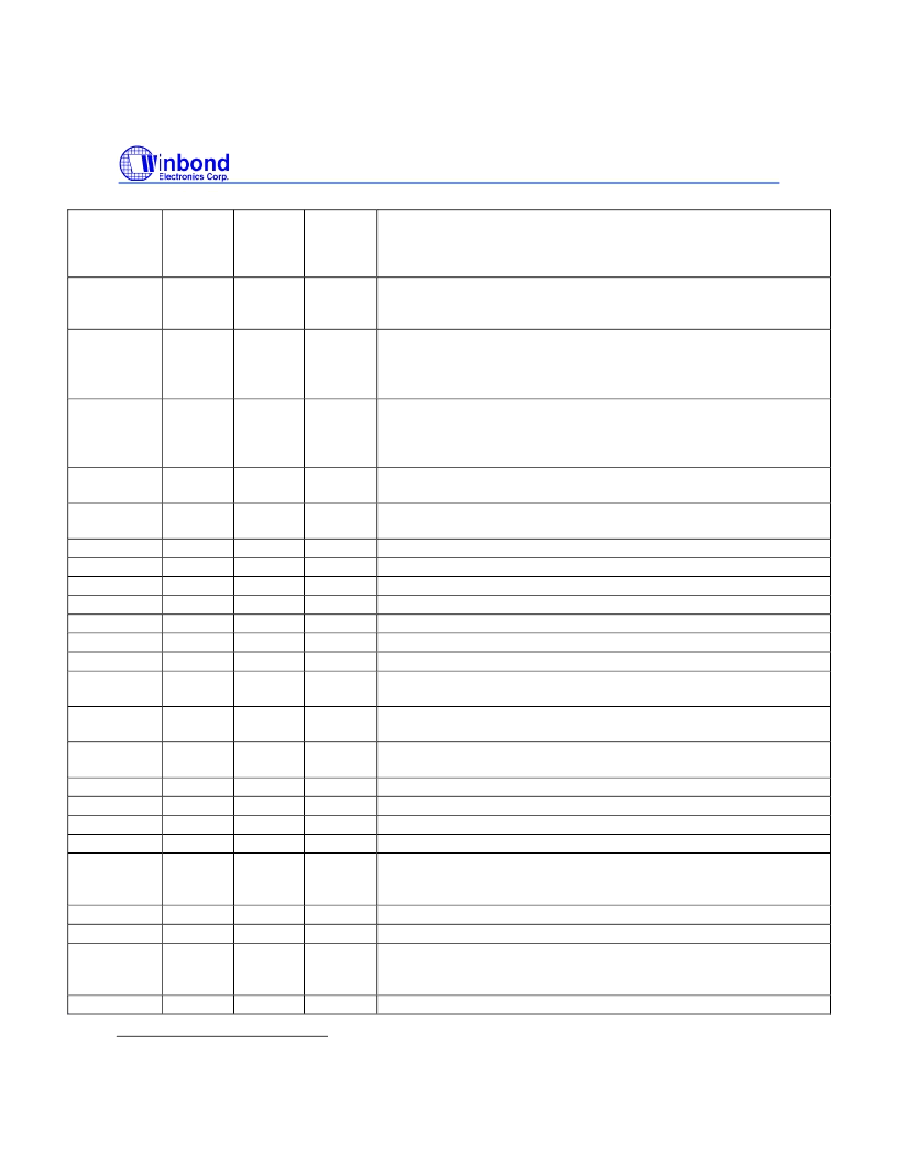
PIN DESCRIPTION
Pin Name
Pin No.
28-pin
TSOP
4
Pin No.
28-pin
PDIP
25
Pin No.
28-pin
SOIC
25
Functionality
RAC
Row Address Clock; an open drain output. The RAC pin goes LOW
T
RACLO
at exactly the end of each row of memory.
Interrupt Output; an open drain output indicating that a set EOM bit
has been found during Playback, or that the chip is in an Overflow
(OVF) condition. This pin remains LOW until a Read Status
command is executed.
This pin allows the internal clock of the Voice record/playback
system to be externally driven for enhanced timing precision. This
pin is grounded for most applications. It is required for the CODEC
operation.
Serial Clock Line is part of the I
2
C serial bus. It is used to clock the
data into and out of the I
2
C interface.
Serial Data Line is part of the I
2
C serial bus. Data is passed
between devices on the bus over this line.
Input pin that supplies the LSB for the I
2
C Slave Address.
Input pin that supplies the LSB +1 bit for the I
2
C Slave Address.
Differential positive Input to the microphone amplifier.
Differential negative Input to the microphone amplifier.
Microphone Bias Voltage
AGC Capacitor connection. Required for the on-chip AGC amplifier.
Differential Positive Speaker Driver Output.
Differential Negative Speaker Driver Output. When the speaker
outputs are in use, the AUX OUT output is disabled.
Auxiliary Input. This is one of the gain adjustable analog inputs for
the device.
Auxiliary Output. This is one the analog outputs for the device.
When this output is in use, the SP+ and SP- outputs are disabled.
Serial Digital Audio PCM Input.
Serial Digital Audio PCM Output or I
2
S Input/Output.
Digital audio PCM Frame sync (FS) or I
2
S Word Sync (WS).
Digital audio PCM or I
2
S Serial Clock.
Positive Digital Supply pins. These pins carry noise generated by
internal clocks in the chip. They must be carefully bypassed to
Digital Ground to ensure correct device operation.
Digital Ground pins.
Analog Ground pins.
Positive Analog Supply pin. This pin supplies the low level audio
sections for the device. It should be carefully bypassed to Analog
Ground to ensure correct device operation.
No Connection
before the end of each row of memory, and returns HIGH
/INT
5
26
26
MCLK
6
27
27
SCL
9
2
2
SDA
11
4
4
A0
A1
MIC+
MIC-
MICBS
ACAP
SP+
SP-
12
10
16
17
18
19
22
20
5
3
9
10
11
12
15
13
7
3
10
9
8
12
15
13
AUX IN
24
17
17
AUX OUT
25
18
20
SDI
SDIO
WS
SCK
V
CCD
2
3
28
27
7,8
23
24
21
20
1,28
22
24
18
19
1,28
V
SSD
V
SSA
V
CCA
13,14
1,15,21
23
6,7
5,6
8,14,22
16
11,14,23
16
NC
26
19
21
1
See parameters section of the datasheet.
相關(guān)PDF資料 |
PDF描述 |
|---|---|
| I5216X | 8 TO 16 MINUTE VOICE RECORD/PLAYBACK SYSTEM WITH INTEGRATED CODEC |
| I7032 | 200 Mbps Laser-Diode Driver |
| I7032-EN | 200 Mbps Laser-Diode Driver |
| I7032-ET | 200 Mbps Laser-Diode Driver |
| I7110 | 300 Mbps LED Drivers |
相關(guān)代理商/技術(shù)參數(shù) |
參數(shù)描述 |
|---|---|
| I5216X | 制造商:WINBOND 制造商全稱:Winbond 功能描述:8 TO 16 MINUTE VOICE RECORD/PLAYBACK SYSTEM WITH INTEGRATED CODEC |
| I521-7J3-20.000 | 制造商:ILSI 制造商全稱:ILSI America LLC 功能描述:Surface Mount Oscillator, TCXO, TCVCXO Metal Package, 11 mm x 18 mm |
| I521-7J5-20.000 | 制造商:ILSI 制造商全稱:ILSI America LLC 功能描述:Surface Mount Oscillator, TCXO, TCVCXO Metal Package, 11 mm x 18 mm |
| I521-7O3-20.000 | 制造商:ILSI 制造商全稱:ILSI America LLC 功能描述:Surface Mount Oscillator, TCXO, TCVCXO Metal Package, 11 mm x 18 mm |
| I521-7O5-20.000 | 制造商:ILSI 制造商全稱:ILSI America LLC 功能描述:Surface Mount Oscillator, TCXO, TCVCXO Metal Package, 11 mm x 18 mm |
發(fā)布緊急采購,3分鐘左右您將得到回復(fù)。