- 您現(xiàn)在的位置:買賣IC網(wǎng) > PDF目錄371907 > HWD2108 (Electronic Theatre Controls, Inc.) Dual 105 mW Headphone Amplifier PDF資料下載
參數(shù)資料
| 型號: | HWD2108 |
| 廠商: | Electronic Theatre Controls, Inc. |
| 英文描述: | Dual 105 mW Headphone Amplifier |
| 中文描述: | 雙105毫瓦耳機放大器 |
| 文件頁數(shù): | 3/18頁 |
| 文件大小: | 944K |
| 代理商: | HWD2108 |
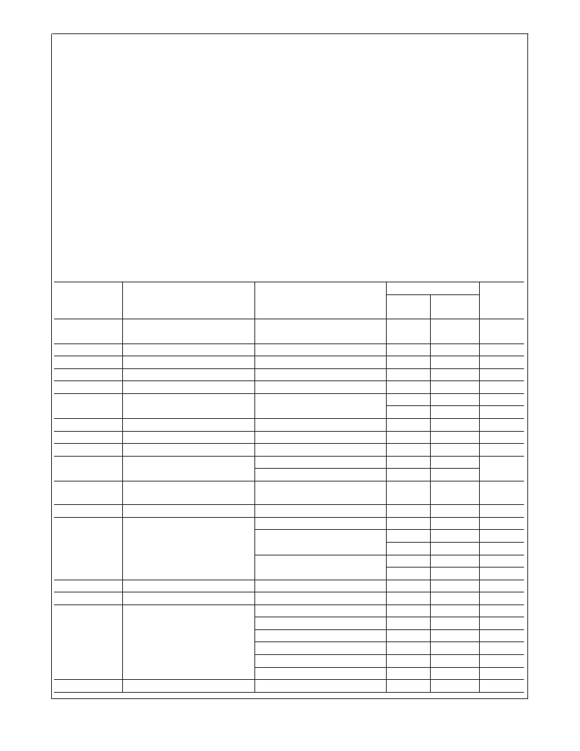
Absolute Maximum Ratings
If Military/Aerospace specified devices are required,
please contact the
CSMSC
Semiconductor Sales Office/
Distributors for availability and specifications.
(Note 3)
Supply Voltage
Storage Temperature
Input Voltage
Power Dissipation (Note 4)
ESD Susceptibility (Note 5)
ESD Susceptibility (Note 6)
Junction Temperature
Soldering Information (Note 1)
Small Outline Package
Vapor Phase (60 seconds)
Infrared (15 seconds)
Thermal Resistance
6.0V
65C to +150C
0.3V to V
DD
+ 0.3V
Internally limited
3500V
250V
150C
215C
220C
θ
JC
(MSOP)
θ
JA
(MSOP)
θ
JC
(SOP)
θ
JA
(SOP)
θ
JC
(LLP)
θ
JA
(LLP)
θ
JA
(LLP)
56C/W
210C/W
35C/W
170C/W
15C/W
117C/W (Note 9)
150C/W (Note 10)
Operating Ratings
Temperature Range
T
MIN
≤
T
A
≤
T
MAX
Supply Voltage
40C
≤
T
A
≤
85C
2.0V
≤
V
DD
≤
5.5V
Note 1:
See AN-450 “Surface Mounting and their Effects on Product Reli-
ability” for other methods of soldering surface mount devices.
Electrical Characteristics
(Notes 2, 3)
The following specifications apply for V
DD
= 5V unless otherwise specified, limits apply to T
A
= 25C.
Symbol
Parameter
Conditions
HWD21
08
Limit
(Note
Units
(Limits)
Typ
(Note
7)
8)
2.0
5.5
3.0
16.5
50
V
DD
Supply Voltage
V (min)
V (max)
mA (max)
mW (max)
mV (max)
pA
V
V
dB
mA
I
DD
P
tot
V
OS
Ibias
Supply Current
Total Power Dissipation
Input Offset Voltage
Input Bias Current
V
IN
= 0V, I
O
= 0A
V
IN
= 0V, I
O
= 0A
V
IN
= 0V
1.2
6
10
10
0
4.3
67
70
0.1
.3
4.7
89
V
CM
Common Mode Voltage
G
V
Io
R
O
V
O
Open-Loop Voltage Gain
Max Output Current
Output Resistance
Output Swing
R
L
= 5k
THD+N
<
0.1 %
R
L
= 32
, 0.1% THD+N, Min
R
L
= 32
, 0.1% THD+N, Max
Cb = 1.0μF, Vripple = 100mV
PP
,
f = 100Hz
R
L
= 32
f = 1 kHz
R
L
= 16
,
V
O
=3.5V
PP
(at 0 dB)
R
L
= 32
,
V
O
=3.5V
PP
(at 0 dB)
V
O
= 3.5V
pp
(at 0 dB)
Open Loop, R
L
= 5k
THD+N = 0.1%, f = 1 kHz
R
L
= 16
R
L
= 32
THD+N = 10%, f = 1 kHz
R
L
= 16
R
L
= 32
V
PSRR
Power Supply Rejection Ratio
dB
Crosstalk
THD+N
Channel Separation
Total Harmonic Distortion + Noise
75
dB
0.05
66
0.05
66
105
5.5
%
dB
%
dB
dB
MHz
SNR
f
G
P
o
Signal-to-Noise Ratio
Unity Gain Frequency
Output Power
105
70
mW
mW
60
150
90
3
mW
mW
pF
C
I
Input Capacitance
3
相關(guān)PDF資料 |
PDF描述 |
|---|---|
| HWD2182 | 250mW Audio Power Amplifier with Shutdown Mode |
| HWF1682RA | L-Band GaAs Power FET |
| HWF1687RA | L-Band GaAs Power FET |
| HWL36YRA | L-Band GaAs Power FET |
| HWS2152 | GaAs MMIC SPDT Switch |
相關(guān)代理商/技術(shù)參數(shù) |
參數(shù)描述 |
|---|---|
| HWD2111 | 制造商:未知廠家 制造商全稱:未知廠家 功能描述:Dual 105mW Headphone Amplifier with Digital Volume Control and Shutdown Mode |
| HWD2119 | 制造商:未知廠家 制造商全稱:未知廠家 功能描述:350mWAudio Power Amplifier with Shutdown Mode |
| HWD2171 | 制造商:未知廠家 制造商全稱:未知廠家 功能描述:低電壓放大器 |
| HWD2182 | 制造商:未知廠家 制造商全稱:未知廠家 功能描述:250mW Audio Power Amplifier with Shutdown Mode |
| HWD2190 | 制造商:未知廠家 制造商全稱:未知廠家 功能描述:1 Watt Audio Power Amplifier |
發(fā)布緊急采購,3分鐘左右您將得到回復(fù)。