- 您現(xiàn)在的位置:買(mǎi)賣(mài)IC網(wǎng) > PDF目錄385409 > HV111 (Supertex, Inc.) Inrush Limiter/Circuit Breaker/Hotswap Controller IC PDF資料下載
參數(shù)資料
| 型號(hào): | HV111 |
| 廠商: | Supertex, Inc. |
| 元件分類(lèi): | 脈沖抑制器 |
| 英文描述: | Inrush Limiter/Circuit Breaker/Hotswap Controller IC |
| 中文描述: | 浪涌電流限制器/斷路器/熱插拔控制器IC |
| 文件頁(yè)數(shù): | 7/9頁(yè) |
| 文件大?。?/td> | 551K |
| 代理商: | HV111 |

HV111
Description of Operation
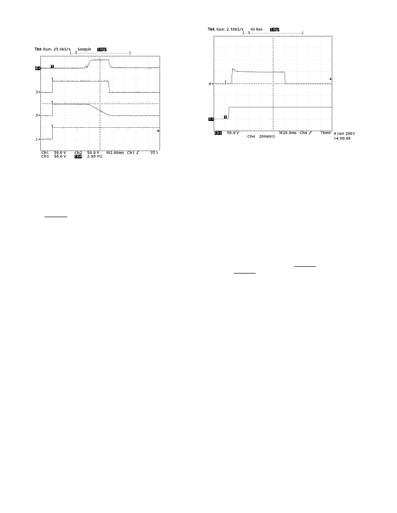
Figure 9 – Turn on Waveforms
I
DS
I
DS
V
PGRND
-V
NN
V
DRAIN
-V
NN
V
DRAIN
-V
NN
V
PP
-V
NN
Initial Inrush Timeout
Figure 10 – Limit Timeout
The HV111 monitors the drain source voltage and the output
current. During hotswap if the drain source does not drop
below 1/4 of input voltage within a shorted-circuit timer
period (t
= 75ms), then the part will conclude that a short
circuit condition exists, will turn off the internal MOSFET and
auto-retry with a period of 9.0sec. This case is illustrated in
Fig. 10 above (where waveform 4 is DRAIN current and
waveform 1 is V
). Note that if the short circuit is low
enough impedance to hold the DRAIN voltage within ~1V of
V
then the PWM current limit will engage as shown in Fig.
7. Further, the PWM current limit will remain until
V
PP
– V
DS
>~1V.
After the hotswap period is finished successfully, the internal
MOSFET is turned fully on & the PWRGD bar is pulled low
(ACTIVE). PWRGD bar operation (connected to a pullup) is
illustrated by Waveform 3 in Fig. 9.
Referring to Figure 9, the operation of the HV111 may be
illustrated. On initial power application (waveform 1 in
Fig. 9) the HV111 provides a regulated supply for the
internal circuitry. Until the proper internal voltage is achieved
all circuits are held reset, the N-channel MOSFET is off and
the PWRGD bar pin is open (INACTIVE). Once the internal
regulator is safe to operate, the under voltage lock out
(UVLO) senses the input voltage. The UVLO will hold the
pass element off until it is satisfied. At any time during the
start up cycle or thereafter, the input voltage falling below
the UVLO threshold will turn off the N-channel MOSFET and
reset all internal circuitry. The IC also includes a clamp for
the spurious inrush through Cload and the Cfb of the
MOSFET pass element. A normal restart sequence will be
initiated once the input voltage rises above the UVLO
threshold.
The UVLO supervisor works in conjunction with a power on
reset (POR) timer. The timer is approximately 4.5ms to
overcome contact bounce. During the contact bounce if
input voltage falls below the UVLO threshold voltage then
the POR timer will reset. In this way the card will be held off
until bouncing ends. The POR timer will restart again when
the input voltage rises above the UVLO threshold once
again. After a full POR period is satisfied, the N-channel
MOSFET begins to turn on to charge the output capacitor
with a current source limited to ~1.2A (illustrated by
Waveform 4 in Fig. 9). Note the PWM protection at the
leading edge of the current rise in Waveform 4; this is the
PWM protection limiting current because a capacitor initially
appears as a dead short. Waveform 2 shows the V
DS
or
DRAIN pin.
7
相關(guān)PDF資料 |
PDF描述 |
|---|---|
| HV111K4 | Inrush Limiter/Circuit Breaker/Hotswap Controller IC |
| HV219 | Low Charge Injection 8-Channel High Voltage Analog Switch |
| HV219FG | Low Charge Injection 8-Channel High Voltage Analog Switch |
| HV219PJ | Low Charge Injection 8-Channel High Voltage Analog Switch |
| HV219X | Low Charge Injection 8-Channel High Voltage Analog Switch |
相關(guān)代理商/技術(shù)參數(shù) |
參數(shù)描述 |
|---|---|
| HV111K4 | 功能描述:熱插拔功率分布 3/1 Controller IC RoHS:否 制造商:Texas Instruments 產(chǎn)品:Controllers & Switches 電流限制: 電源電壓-最大:7 V 電源電壓-最小:- 0.3 V 工作溫度范圍: 功率耗散: 安裝風(fēng)格:SMD/SMT 封裝 / 箱體:MSOP-8 封裝:Tube |
| HV113SM-12 | 制造商:SPECTRUM 制造商全稱(chēng):Spectrum Microwave, Inc. 功能描述:Voltage Controlled Oscillator |
| HV113T-1 | 制造商:SPECTRUM 制造商全稱(chēng):Spectrum Microwave, Inc. 功能描述:Voltage Controlled Oscillator |
| HV116 | 制造商:Apex Tool Group 功能描述:1 IN. X 16 FT HI-VIZ ORANGE SERIES POWER RETURN TAPE |
| HV12 | 制造商:SEMTECH_ELEC 制造商全稱(chēng):SEMTECH ELECTRONICS LTD. 功能描述:FAST RECOVERY HIGH VOLTAGE DIODES |
發(fā)布緊急采購(gòu),3分鐘左右您將得到回復(fù)。