- 您現(xiàn)在的位置:買賣IC網(wǎng) > PDF目錄385405 > HT86384 (Holtek Semiconductor Inc.) Voice Synthesizer 8-Bit MCU PDF資料下載
參數(shù)資料
| 型號: | HT86384 |
| 廠商: | Holtek Semiconductor Inc. |
| 英文描述: | Voice Synthesizer 8-Bit MCU |
| 中文描述: | 語音合成器8位微控制器 |
| 文件頁數(shù): | 23/39頁 |
| 文件大小: | 368K |
| 代理商: | HT86384 |
第1頁第2頁第3頁第4頁第5頁第6頁第7頁第8頁第9頁第10頁第11頁第12頁第13頁第14頁第15頁第16頁第17頁第18頁第19頁第20頁第21頁第22頁當(dāng)前第23頁第24頁第25頁第26頁第27頁第28頁第29頁第30頁第31頁第32頁第33頁第34頁第35頁第36頁第37頁第38頁第39頁

HT86XXX
Rev. 1.70
23
May 6, 2004
RegisterBit No. Label
Function
INTCH
(1EH)
0
ET2I
Controls the timer 2 interrupt
(1= enabled; 0= disabled)
1
ET3I
Controls the timer 3 interrupt
(1= enabled; 0= disabled)
2, 3
Unused bit, read as 0
4
T2F
Timer 2 interrupt request flag
(1= active; 0= inactive)
5
T3F
Timer 3 interrupt request flag
(1= active; 0= inactive)
6, 7
Unused bit, read as 0
INTC1 Register
Interrupt Source
Priority
Vector
External Interrupt
1
04H
Timer/Event Counter 0 Overflow
2
08H
Timer/Event Counter 1 Overflow
3
0CH
Timer Counter 2 Overflow
4
10H
Timer Counter 3 Overflow
5
14H
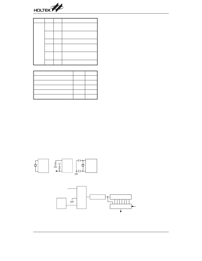
Oscillator Configuration
The HT86XXX provides two types of oscillator circuit for
the system clock, i.e., RC oscillator and crystal oscilla-
tor. No matter what type of oscillator, the signal is used
for the system clock. The HALT mode stops the system
oscillatorandignoresexternalsignaltoconservepower.
If the RC oscillator is used, an external resistor between
OSC1 and VSS is required, and the range of the resis-
tance should be from 30k
divided by 4, is available on OSC2 with pull-high resis-
tor, which can be used to synchronize external logic.
The RC oscillator provides the most cost effective solu-
tion. However, the frequency of the oscillation may vary
to 680k . The system clock,
with VDD, temperature, and the chip itself due to pro-
cess variations. It is therefore not suitable for timing
sensitive operations where accurate oscillator fre-
quency is desired.
On the other hand, if the crystal oscillator is selected, a
crystalacrossOSC1andOSC2isneededtoprovidethe
feedback and phase shift required for the oscillator, and
no other external components are required. Aresonator
may be connected between OSC1 and OSC2 to replace
the crystal and to get a frequency reference, but two ex-
ternal capacitors in OSC1 and OSC2 are required.
There is another oscillator circuit designed for Timer3 s
clock source as the RTC time base which is determined
by mask option. If the mask option determines that
Timer3 s clock source is from a 32kHz crystal, then a
32kHz crystal should be connected to XIN and XOUT.
Watchdog Timer
WDT
The WDT clock source is implemented by a dedicated
RC oscillator (WDT oscillator) or instruction clock (sys-
tem clock divided by 4), decided by mask options. This
timer is designed to prevent a software malfunction or
sequence jumping to an unknown location with unpre-
dictable results. The Watchdog Timer can be disabled
by mask option. If the Watchdog Timer is disabled, all
theexecutionsrelatedtotheWDTresultinnooperation.
Once the internal WDT oscillator (RC oscillator with pe-
riod 78 s normally) is selected, it is first divided by 256
(8-stages) to get the nominal time-out period of approxi-
mately 20 ms. This time-out period may vary with tem-
perature, VDD and process variations. By invoking the
WDT prescaler, longer time-out period can be realized.
Writing data to WS2, WS1, WS0 (bit 2,1,0 of
WDTS(09H)) can give different time-out period.
If WS2, WS1, WS0 all equal to 1, the division ratio is up
to 1:128, and the maximum time-out period is 2.6 sec-
onds.
If the device operates in a noisy environment, using the
on-chip RC oscillator (WDT OSC) is strongly recom-
mended, since the HALT will stop the system clock.
"
- '
- -
'
- -
%
&
) *
'
- -
7
. 8
System Oscillator
"
'
-
> ) *
4 9 /
'
,
'
-
1 9 /
'
4 9
9 '
,
'
9
,
2 ,
>
-
,
Watchdog Timer
相關(guān)PDF資料 |
PDF描述 |
|---|---|
| HT86576 | Voice Synthesizer 8-Bit MCU |
| HT86R192 | Voice Synthesizer 8-Bit OTP MCU |
| HT86R384 | Voice Synthesizer 8-Bit OTP MCU |
| HT86XXX | 8-Bit Voice Synthesizer MCU |
| HT8950 | Voice Modulator |
相關(guān)代理商/技術(shù)參數(shù) |
參數(shù)描述 |
|---|---|
| HT86384(68PLCC) | 制造商:未知廠家 制造商全稱:未知廠家 功能描述:Microcontroller |
| HT8650 | 制造商:未知廠家 制造商全稱:未知廠家 功能描述:IC-MESSAGE REMINDER IC |
| HT8650(28DIP) | 制造商:未知廠家 制造商全稱:未知廠家 功能描述:Speech Synthesizer |
| HT8650(28SDIP) | 制造商:未知廠家 制造商全稱:未知廠家 功能描述:Speech Synthesizer |
| HT8650(28SOIC) | 制造商:未知廠家 制造商全稱:未知廠家 功能描述:Speech Synthesizer |
發(fā)布緊急采購,3分鐘左右您將得到回復(fù)。