- 您現(xiàn)在的位置:買賣IC網(wǎng) > PDF目錄385401 > HT6750A (Holtek Semiconductor Inc.) Date Printer PDF資料下載
參數(shù)資料
| 型號: | HT6750A |
| 廠商: | Holtek Semiconductor Inc. |
| 英文描述: | Date Printer |
| 中文描述: | 日期打印機(jī) |
| 文件頁數(shù): | 3/8頁 |
| 文件大小: | 126K |
| 代理商: | HT6750A |

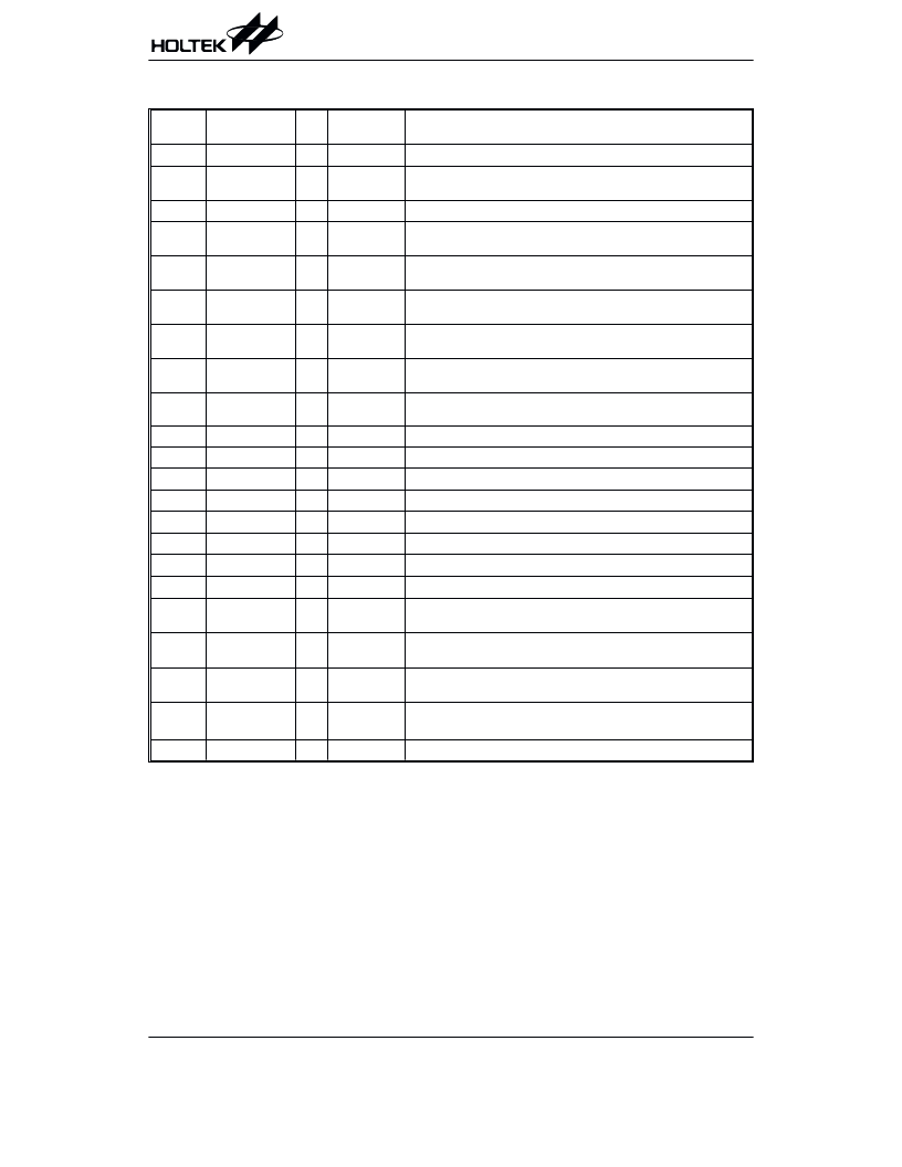
Pad Description
Pad No.
Pad Name
I/O
Internal
Connection
Description
1, 2
VSS
Negative power supply, ground
3,
19, 20
COM1
COM3, COM2
O
CMOS
Output for LCD panel common
4~18
SEG1~SEG15
O
CMOS
LCD segment output driver
21
MODE
I
CMOS with
Pull-high
Mode select input pin (Internal pull-high 75K)
22
SEL
I
CMOS with
Pull-high
Correction digit shift switch (Internal pull-high 75K)
23
SET
I
CMOS with
Pull-high
Correction digit data (Internal pull-high 75K)
24
SEGON
I
CMOS with
Pull-high
Est pin, if pull-low will force all segment ON
25
RESET
I
CMOS with
Pull-low
External Reset input (Internal pull-low, 50K)
26
TEST1
I
CMOS with
Pull-low
Test pin (not for customer)
27
OSCO
O
CMOS
Crystal oscillator output pin
28
OSCI
I
CMOS
Crystal oscillator input pin
29, 30
VDD
Positive power supply
31
VF4
O
CMOS
Double reference voltage
32, 33
LC2, LC1
I
CMOS
Connected to 0.1 F capacitor
34
VF2
O
CMOS
Reference voltage
35~40
RF1~RF6
I
Adjust regulator output voltage, TRIM PIN
41~44
TR1~TR4
I
Adjust constant voltage and drive lamp output pin (Open drain)
45
T
I
CMOS with
Pull-high
Imprint time select input (Internal pull-high 75K with Latch type )
46
D
I
CMOS with
Pull-high
Imprint time external control input (Internal pull-high 75K with
Latch type )
47
X
I
CMOS with
Pull-high
Imprint trigger input pin (Internal pull-high 75K)*
48
TEST2
I
CMOS with
Pull-high
For coustomer test PRINTING LCD use only, pull-low will force
Lamp ON and other function is OK (Internal pull-high 75K)**
49
LAMP
O
CMOS
Drive lamp output pin (Open drain)
Note:
*TheXinputhasnoeffectinOFFmode,selectionandsettingmode;thelampwillbeturnedoffautomatically.
** The TEST2 has no effect in selection and setting mode; the lamp will be turned off automatically.
Absolute Maximum Ratings
Supply Voltage .......................................................5.5V
Storage Temperature ............................ 20 C to 60 C
Input Voltage ......................................................... 5.5V
Operating Temperature...............................0 C to 50 C
StaticElectricity(OFFPower)...................................................................................200pF, 200V,10timestoeachpin
Note: These are stress ratings only. Stresses exceeding the range specified under Absolute Maximum Ratings may
cause substantial damage to the device. Functional operation of this device at other conditions beyond those
listed in the specification is not implied and prolonged exposure to extreme conditions may affect device reliabil-
ity.
HT6750A
Rev. 1.00
3
January 17, 2003
相關(guān)PDF資料 |
PDF描述 |
|---|---|
| HT6751A | Camera Motor Driver (1.5 Channel)(照相機(jī)電機(jī)驅(qū)動器(1.5 通道)) |
| HT6751B | Camera Motor Driver (1.5 Channel)(照相機(jī)電機(jī)驅(qū)動器(1.5 通道)) |
| HT682L | 318 Series of Decoders |
| HT605L | 318 Series of Decoders |
| HT612 | 318 Series of Decoders |
相關(guān)代理商/技術(shù)參數(shù) |
參數(shù)描述 |
|---|---|
| HT6751A | 制造商:HOLTEK 制造商全稱:Holtek Semiconductor Inc 功能描述:Camera Motor Driver (1.5 Channel) |
| HT6751B | 制造商:HOLTEK 制造商全稱:Holtek Semiconductor Inc 功能描述:Camera Motor Driver (1.5 Channel) |
| HT67F30 | 制造商:HOLTEK 制造商全稱:Holtek Semiconductor Inc 功能描述:TinyPowerTM A/D Flash Type 8-Bit MCU with LCD & EEPROM |
| HT67F40 | 制造商:HOLTEK 制造商全稱:Holtek Semiconductor Inc 功能描述:TinyPowerTM A/D Flash Type 8-Bit MCU with LCD & EEPROM |
| HT67F50 | 制造商:HOLTEK 制造商全稱:Holtek Semiconductor Inc 功能描述:TinyPowerTM A/D Flash Type 8-Bit MCU with LCD & EEPROM |
發(fā)布緊急采購,3分鐘左右您將得到回復(fù)。