- 您現在的位置:買賣IC網 > PDF目錄385399 > HT46C47 (Holtek Semiconductor Inc.) Cost-Effective A/D Type 8-Bit MCU PDF資料下載
參數資料
| 型號: | HT46C47 |
| 廠商: | Holtek Semiconductor Inc. |
| 英文描述: | Cost-Effective A/D Type 8-Bit MCU |
| 中文描述: | 成本效益的A / D型8位微控制器 |
| 文件頁數: | 3/42頁 |
| 文件大?。?/td> | 291K |
| 代理商: | HT46C47 |
第1頁第2頁當前第3頁第4頁第5頁第6頁第7頁第8頁第9頁第10頁第11頁第12頁第13頁第14頁第15頁第16頁第17頁第18頁第19頁第20頁第21頁第22頁第23頁第24頁第25頁第26頁第27頁第28頁第29頁第30頁第31頁第32頁第33頁第34頁第35頁第36頁第37頁第38頁第39頁第40頁第41頁第42頁

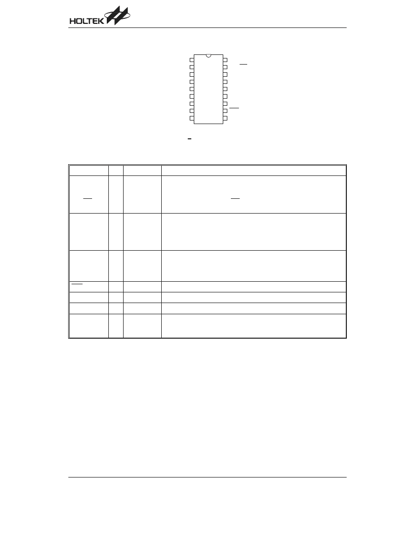
Pin Assignment
Pin Description
Pin Name
I/O
Options
Description
PA0~PA2
PA3/PFD
PA4/TMR
PA5/INT
PA6, PA7
I/O
Pull-high
Wake-up
PA3 or PFD
Bidirectional 8-bit input/output port. Each bit can be configured as wake-up
input by options. Software instructions determine the CMOS output or Schmitt
triggerinputwithorwithoutpull-highresistor(determinedbypull-highoptions:bit
option). The PFD, TMR and INT are pin-shared with PA3, PA4 and PA5, re-
spectively.
PB0/AN0
PB1/AN1
PB2/AN2
PB3/AN3
I/O
Pull-high
Bidirectional 4-bit input/output port. Software instructions determine the
CMOS output, Schmitt trigger input with or without pull-high resistor (deter-
mined by pull-high options: bit option) or A/D input.
Once a PB line is selected as an A/D input (by using software control), the I/O
function and pull-high resistor are disabled automatically.
PD0/PWM
I/O
Pull-high
PD0 or PWM
Bidirectional I/O line. Software instructions determine the CMOS output,
Schmitt trigger input with or without a pull-high resistor (determined by
pull-high options: bit option). The PWM output function is pin-shared with
PD0 (dependent on PWM options).
RES
I
Schmitt trigger reset input. Active low.
VDD
Positive power supply
VSS
Negative power supply, ground.
OSC1
OSC2
I
O
Crystal
or RC
OSC1, OSC2 are connected to an RC network or a Crystal (determined by
options) for the internal system clock. In the case of RC operation, OSC2 is
the output terminal for 1/4 system clock.
Absolute Maximum Ratings
Supply Voltage...........................V
SS
0.3V to V
SS
+6.0V
Storage Temperature............................ 50 C to 125 C
Input Voltage..............................V
SS
0.3V to V
DD
+0.3V
Operating Temperature........................... 40 C to 85 C
Note: These are stress ratings only. Stresses exceeding the range specified under Absolute Maximum Ratings may
cause substantial damage to the device. Functional operation of this device at other conditions beyond those
listed in the specification is not implied and prolonged exposure to extreme conditions may affect device reliabil-
ity.
HT46R46/HT46C46/HT46R47/HT46C47
Rev. 1.00
3
December 28, 2004
5
6
1
+
,
-
1
,
,
1
1
7
6
5
,
1
,
5
6
7
8
相關PDF資料 |
PDF描述 |
|---|---|
| HT46R46 | Cost-Effective A/D Type 8-Bit MCU |
| HT46C62 | A/D with LCD Type 8-Bit MCU |
| HT46R62 | A/D with LCD Type 8-Bit MCU |
| HT46C63 | A/D with LCD Type 8-Bit MCU |
| HT46C63-100QEP-A | A/D with LCD Type 8-Bit MCU |
相關代理商/技術參數 |
參數描述 |
|---|---|
| HT46C47E | 制造商:HOLTEK 制造商全稱:Holtek Semiconductor Inc 功能描述:Cost-Effective A/D Type 8-Bit MCU |
| HT46C48A | 制造商:HOLTEK 制造商全稱:Holtek Semiconductor Inc 功能描述:Cost-Effective A/D Type 8-Bit MCU |
| HT46C48AE | 制造商:HOLTEK 制造商全稱:Holtek Semiconductor Inc 功能描述:Cost-Effective A/D Type 8-Bit MCU |
| HT46C62 | 制造商:HOLTEK 制造商全稱:Holtek Semiconductor Inc 功能描述:A/D with LCD Type 8-Bit MCU |
| HT46C63 | 制造商:HOLTEK 制造商全稱:Holtek Semiconductor Inc 功能描述:A/D with LCD Type 8-Bit MCU |
發(fā)布緊急采購,3分鐘左右您將得到回復。