- 您現(xiàn)在的位置:買賣IC網(wǎng) > PDF目錄385398 > HT27LC020 (Holtek Semiconductor Inc.) OTP CMOS 256Kx 8-Bit EPROM PDF資料下載
參數(shù)資料
| 型號: | HT27LC020 |
| 廠商: | Holtek Semiconductor Inc. |
| 英文描述: | OTP CMOS 256Kx 8-Bit EPROM |
| 中文描述: | 檢察官辦公室的CMOS 256Kx 8位存儲器 |
| 文件頁數(shù): | 6/15頁 |
| 文件大小: | 203K |
| 代理商: | HT27LC020 |
HT27LC020
Rev. 1.50
6
December 8, 2003
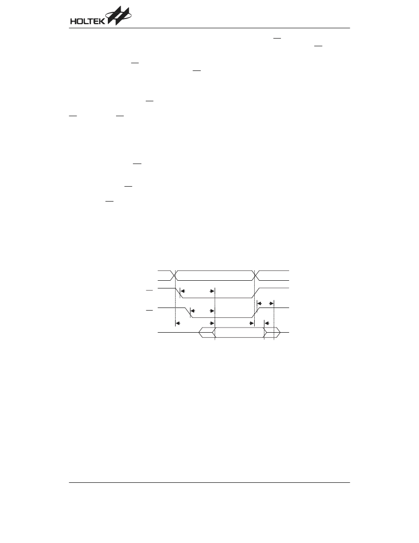
Read Mode
The HT27LC020 has two control functions, both of
which must be logically satisfied in order to obtain data
at outputs. Chip Enable (CE) is the power control and
should be used for device selection. Output Enable (OE)
is the output control and should be used to gate data to
the output pins, independent of device selection. As-
suming that addresses are stable, address access time
(t
ACC
) is equal to the delay from CE to output (t
CE
). Data
is available at the outputs (t
OE
) after the falling edge of
OE, assuming the CE has been LOW and addresses
have been stable for at least t
ACC
t
OE
.
Standby Mode
The HT27LC020 has CMOS standby mode which re-
duces the maximum VCC current to 10 A. It is placed in
CMOS standby when CE is at V
CC
0.3V. The
HT27LC020 also has a TTL-standby mode which re-
duces the maximum VCC current to 0.6mA. It is placed
in TTL-standby when CE is at V
IH
. When in standby
mode, the outputs are in a high-impedance state, inde-
pendent of the OE input.
Two-line Output Control Function
To accommodate multiple memory connections, a
two-line control function is provided to allow for:
Low memory power dissipation
Assurance that output bus contention will not occur
It is recommended that CE be decoded and used as the
primary device-selection function, while OE be made a
common connection to the READ line from the system
control bus. This assures that all deselected memory
devices are in their low-power standby mode and that
theoutputpinsareonlyactivewhendataisdesiredfrom
a particular memory device.
System Considerations
During the switch between active and standby condi-
tions, transient current peaks are produced on the rising
and falling edges of Chip Enable. The magnitude of
these transient current peaks is dependent on the out-
put capacitance loading of the device. At a minimum, a
0.1 F ceramic capacitor (high frequency, low inherent
inductance) should be used on each device between
VCC and VPP to minimize transient effects. In addition,
to overcome the voltage drop caused by the inductive
effects of the printed circuit board traces on EPROM ar-
rays, a 4.7 F bulk electrolytic capacitor should be used
between VCC and VPP for each eight devices. The lo-
cation of the capacitor should be close to where the
power supply is connected to the array.
# #
# # &
9 :
9
;
&
9
<
Figure 1. A.C. Waveforms for Read Operation
相關(guān)PDF資料 |
PDF描述 |
|---|---|
| HT27LC040 | CMOS 512K 8-Bit OTP EPROM |
| HT27LC512 | OTP CMOS 64Kx 8-Bit EPROM |
| HT2812 | Single Sound Generator |
| HT2812-14DIP | Single Sound Generator |
| HT2812-8DIP | Single Sound Generator |
相關(guān)代理商/技術(shù)參數(shù) |
參數(shù)描述 |
|---|---|
| HT27LC020-32DIP | 制造商:未知廠家 制造商全稱:未知廠家 功能描述:x8 EPROM |
| HT27LC020-32PLCC | 制造商:未知廠家 制造商全稱:未知廠家 功能描述:x8 EPROM |
| HT27LC020-32SOP | 制造商:未知廠家 制造商全稱:未知廠家 功能描述:x8 EPROM |
| HT27LC040 | 制造商:HOLTEK 制造商全稱:Holtek Semiconductor Inc 功能描述:CMOS 512K 8-Bit OTP EPROM |
| HT27LC4096 | 制造商:未知廠家 制造商全稱:未知廠家 功能描述:CMOS 256K?16-Bit OTP EPROM ??(3.3V) |
發(fā)布緊急采購,3分鐘左右您將得到回復(fù)。