- 您現(xiàn)在的位置:買賣IC網(wǎng) > PDF目錄384443 > HSP48212 (Intersil Corporation) Digital Video Mixer PDF資料下載
參數(shù)資料
| 型號(hào): | HSP48212 |
| 廠商: | Intersil Corporation |
| 英文描述: | Digital Video Mixer |
| 中文描述: | 數(shù)字視頻混合器 |
| 文件頁數(shù): | 6/9頁 |
| 文件大?。?/td> | 57K |
| 代理商: | HSP48212 |
6
The BYPASS control signal enables the programmable delay
registers to be bypassed. When BYPASS is high, the delay
control word is forced to all 0’s and no additional delays are
included in any of the input paths. However, when BYPASS
is low, the LD/DEL serial delay control word interface is
active and the delay control word must be initialized in order
to achieve any meaningful results.
Format Control Signals
The control signals TC and RND0-1 are used to specify the
input data representation and the output data representation
respectively. TC and RND0-1 are synchronous to CLK,
which allows them to be changed on a cycle by cycle basis if
needed. The control signals are designed to match the
latency of the data paths. When the control inputs change,
the new configuration will effect the current input data and
will not effect the data in the pipeline stages. For example, if
the rounding selection is changed from 8-bit rounding to 10-
bit rounding on a given cycle, the output will remain in an 8-
bit representation while the new data is propagating through
the circuit. When the results of the new data are available at
the output, the number format will change to 10-bits.
The RND0-1 control signals determine the number of
significant bits on the output bus DOUT0-12. The output
data may be rounded to 8, 10, 12, or 13-bits. The rounding
operation is performed by adding a binary 1 to the bit
position right of the desired LSB and forcing the undesired
bits to 0. For example, in 8-bit rounding, a 1 is added to the
9th bit to the right of the MSB (DOUT4), and DOUT0-4 are
forced to 0 (i.e., DOUT0-12 = XXXXXXXX00000).
Output Control
DOUT0-12 is the output data bus which represents the
weighted average of the incoming pixel data as indicated by
(EQ. 2):
The output data will be represented in either two’s
complement format or in unsigned format depending on the
value of the TC signal when the input data (DINA0-11 and
DINB0-11) is sampled by CLK. Similarly, the output
representation of DOUT0-12 is also dependent on the value
of RND0-1 during sampling of the input data.
The output data DOUT0-12 is registered at the output of the
HSP48212 on the rising edge of CLK. The output data may
be accessed through the activation of the signal OE. OE is
an asynchronous input which, when low, causes the
DOUT0-12 bus to drive; when OE is high, the DOUT0-12
bus is not driven (floating).
TABLE 1.
INPUT SIGNAL
CONTROL WORD BIT POSITION
RND0-1
12-14
TC
9-11
M0-11
6-8y
DINB0-11
3-5
DINA0-11
0-2
D
C
Q
D
C
Q
D
C
Q
D
C
Q
D
C
Q
D
C
Q
D
C
Q
D
C
Q
D
C
Q
D
C
Q
D
C
Q
D
C
Q
D
C
Q
D
C
Q
D
C
Q
D0
D1
D2
D3
D4
D5
D6
D7
D8
D9
D10
D11
D12
D13
D14
LD
DEL
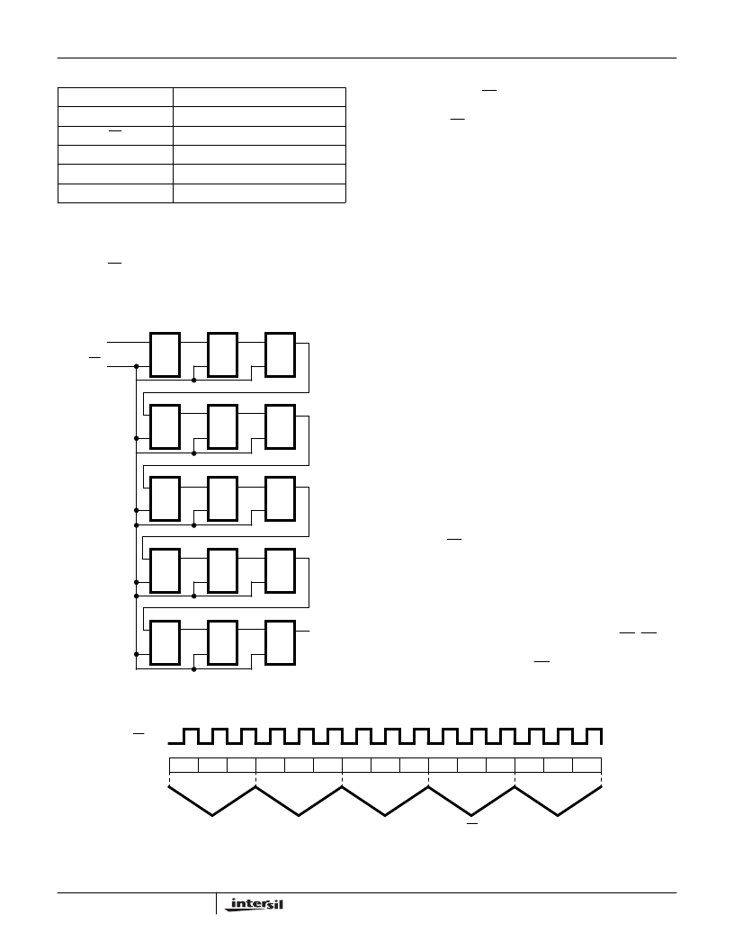
FIGURE 2. DELAY CONTROL WORD SHIFT REGISTER
DOUT = 2 x
DINA x M
(
)
+ DINB x 1 - M
)
)
[
]
(EQ. 2)
D14
D13
D12
D11
D10
D9
D8
D7
D6
D5
D4
D3
D2
D1
D0
DINA
DELAY
DINB
DELAY
MIX
DELAY
RND
DELAY
TC
DELAY
LD
DEL
FIGURE 3. DELAY CONTROL WORD TIMING DIAGRAM
HSP48212
相關(guān)PDF資料 |
PDF描述 |
|---|---|
| HSP48212JC-40 | Digital Video Mixer |
| HSP48212VC-40 | Digital Video Mixer |
| HSP50210JI-52 | Digital Costas Loop |
| HSP50210JC-52 | Digital Costas Loop |
| HSP50216KI | Four-Channel Programmable Digital DownConverter |
相關(guān)代理商/技術(shù)參數(shù) |
參數(shù)描述 |
|---|---|
| HSP48212 WAF | 制造商:Intersil Corporation 功能描述: |
| HSP48212JC-40 | 制造商:Rochester Electronics LLC 功能描述:DIGITAL VIDEO MIXER 68PLCC 40MHZ COMM - Bulk |
| HSP48212VC-40 | 制造商:Harris Corporation 功能描述: 制造商:Intersil Corporation 功能描述: |
| HSP48410 | 制造商:INTERSIL 制造商全稱:Intersil Corporation 功能描述:Histogrammer/Accumulating Buffer |
| HSP48410 WAF | 制造商:Intersil Corporation 功能描述: |
發(fā)布緊急采購,3分鐘左右您將得到回復(fù)。