- 您現(xiàn)在的位置:買賣IC網(wǎng) > PDF目錄384442 > HS1-82C54RH (Intersil Corporation) Radiation Hardened CMOS Programmable Interval Timer PDF資料下載
參數(shù)資料
| 型號: | HS1-82C54RH |
| 廠商: | Intersil Corporation |
| 英文描述: | Radiation Hardened CMOS Programmable Interval Timer |
| 中文描述: | 輻射加固CMOS可編程間隔定時(shí)器 |
| 文件頁數(shù): | 15/21頁 |
| 文件大小: | 171K |
| 代理商: | HS1-82C54RH |
962
HS-82C54RH
Mode Definitions
The following are defined for use in describing the operation
of the HS-82C54RH.
CLK PULSE:
A rising edge, then a falling edge, in that order, of a
Counter’s CLK input.
TRIGGER:
A rising edge of a Counter’s Gate input.
COUNTER LOADING:
The transfer of a count from the CR to the CE (See “Func-
tional Description”)
Mode 0: Interrupt on Terminal Count
Mode 0 is typically used for event counting. After the Control
Word is written, OUT is initially low, and will remain low until
the Counter reaches zero. OUT then goes high and remains
high until a new count or a new Mode 0 Control Word is
written to the Counter.
GATE = 1 enables counting; GATE = 0 disables counting.
GATE has no effect on OUT.
After the Control Word and initial count are written to a
Counter, the initial count will be loaded on the next CLK
pulse. This CLK pulse does not decrement the count, so for
an initial count of N, OUT does not go high until N + 1 CLK
pulses after the initial count is written.
If a new count is written to the Counter it will be loaded on
the next CLK pulse and counting will continue from the new
count. If a two-byte count is written, the following happens:
1. Writing the first byte disables counting. OUT is set low
immediately (no clock pulse required).
2. Writing the second byte allows the new count to be loaded
on next CLK pulse.
This allows the counting sequence to be synchronized by
software. Again OUT does not go high until N + 1 CLK
pulses after the new count of N is written.
If an initial count is written while GATE = 0, it will still
beloaded on the next CLK pulse. When GATE goes high,
OUT will go high N CLK pulses later; no CLK pulse is
needed to load the Counter as this has already been done.
CS
RD
WR
A1
A0
0
1
0
0
0
Write into Counter 0
0
1
0
0
1
Write into Counter 1
0
1
0
1
0
Write into Counter 2
0
1
0
1
1
Write Control Word
0
0
1
0
0
Read from Counter 0
0
0
1
0
1
Read from Counter 1
0
0
1
1
0
Read from Counter 2
0
0
1
1
1
No-Operation (Three-State)
1
X
X
X
X
No-Operation (Three-State)
0
1
1
X
X
No-Operation (Three-State)
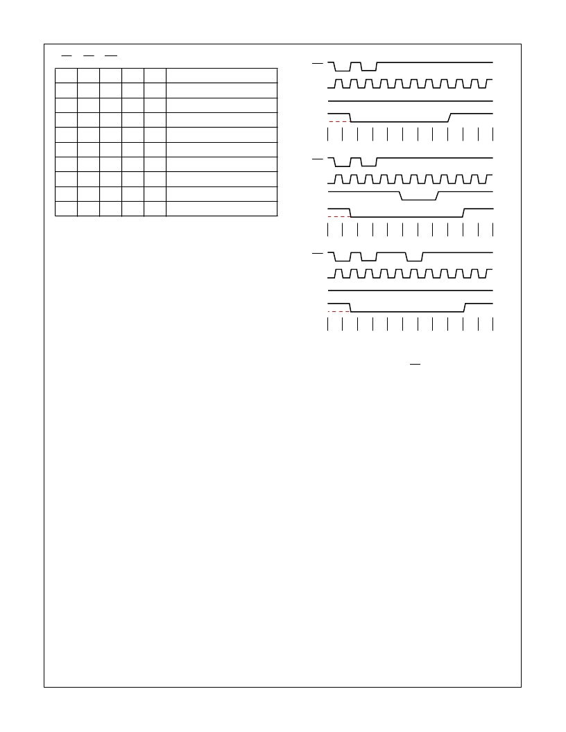
FIGURE 16. READ/WRITE OPERATIONS SUMMARY
NOTES:
1. Counters are programmed for binary (not BCD) counting and for
reading/writing least significant byte (LSB) only.
2. The Counter is always selected (CS always low).
3. CW stands for “Control Word”; CW = 10 means a Control Word
of 10, Hex is written to the Counter.
4. LSB stands for “Least significant byte” of count.
5. Numbers below diagrams are count values. The lower number is
the least significant byte. The upper number is the most signifi-
cant byte. Since the Counter is programmed to read/write LSB
only, the most significant byte cannot be read.
6. N stands for an undefined count.
7. Vertical lines show transitions between count values.
FIGURE 17. MODE 0
Mode 1: Hardware Retriggerable One-Shot
OUT will be initially high. OUT will go low on the CLK pulse
following a trigger to begin the one-shot pulse, and will
remain low until the Counter reaches zero. OUT will then go
high and remain high until the CLK pulse after the next
trigger.
After writing the Control Word and initial count, the Counter
is armed. A trigger results in loading the Counter and setting
OUT low on the next CLK pulse, thus starting the one-shot
pulse N CLK cycles in duration. The one-shot is retrigger-
able, hence OUT will remain low for N CLK pulses after any
trigger. The one-shot pulse can be repeated without rewriting
the same count into the Counter. GATE has no effect on
OUT.
If a new count is written to the Counter during a one-shot
pulse, the current one-shot is not affected unless the
Counter is retriggered. In that case, the Counter is loaded
N
N
N
N
0
3
0
2
0
1
0
0
FF
FF
CW = 10
LSB = 4
WR
CLK
GATE
OUT
N
N
N
N
0
2
0
2
0
2
0
1
0
0
CW = 12
LSB = 3
WR
CLK
GATE
OUT
N
N
N
N
0
2
0
1
0
2
CW = 10
LSB = 3
WR
CLK
GATE
OUT
LSB = 2
0
4
FF
FE
0
3
FF
FF
FF
FF
0
1
0
0
0
3
Spec Number
518059
相關(guān)PDF資料 |
PDF描述 |
|---|---|
| HS9-82C54RH | Radiation Hardened CMOS Programmable Interval Timer |
| HS1-82C54RH-8 | Radiation Hardened CMOS Programmable Interval Timer |
| HS9-82C54RH-8 | Radiation Hardened CMOS Programmable Interval Timer |
| HS1-82C54RH-Q | Radiation Hardened CMOS Programmable Interval Timer |
| HS9-82C54RH-Q | Radiation Hardened CMOS Programmable Interval Timer |
相關(guān)代理商/技術(shù)參數(shù) |
參數(shù)描述 |
|---|---|
| HS1-82C54RH/PROTO | 制造商:Intersil Corporation 功能描述:RAD HARD CMOS PROGRAMMABLE INTERVAL TIMER,PROTO,CLASS V - Rail/Tube |
| HS1-82C54RH-8 | 制造商:Intersil Corporation 功能描述:PROGRAMMABLE TIMER SGL 24PIN SBDIP - Rail/Tube |
| HS1-82C54RH-Q | 制造商:Intersil Corporation 功能描述:PROGRAMMABLE TIMER SGL 24PIN SBCDIP - Rail/Tube |
| HS1-82C55ARH | 制造商:INTERSIL 制造商全稱:Intersil Corporation 功能描述:Radiation Hardened CMOS Programmable Peripheral Interface |
| HS1-82C55ARH-8 | 制造商:Intersil Corporation 功能描述:RAD HARD CMOS PROGRAMMABLE PERIPHERAL INTERFACE,DIP,CLS Q - Rail/Tube |
發(fā)布緊急采購,3分鐘左右您將得到回復(fù)。