- 您現(xiàn)在的位置:買(mǎi)賣(mài)IC網(wǎng) > PDF目錄385388 > HMP8190 (Intersil Corporation) NTSC/PAL Video Encoder PDF資料下載
參數(shù)資料
| 型號(hào): | HMP8190 |
| 廠商: | Intersil Corporation |
| 英文描述: | NTSC/PAL Video Encoder |
| 中文描述: | NTSC / PAL視頻編碼器 |
| 文件頁(yè)數(shù): | 3/32頁(yè) |
| 文件大小: | 227K |
| 代理商: | HMP8190 |
第1頁(yè)第2頁(yè)當(dāng)前第3頁(yè)第4頁(yè)第5頁(yè)第6頁(yè)第7頁(yè)第8頁(yè)第9頁(yè)第10頁(yè)第11頁(yè)第12頁(yè)第13頁(yè)第14頁(yè)第15頁(yè)第16頁(yè)第17頁(yè)第18頁(yè)第19頁(yè)第20頁(yè)第21頁(yè)第22頁(yè)第23頁(yè)第24頁(yè)第25頁(yè)第26頁(yè)第27頁(yè)第28頁(yè)第29頁(yè)第30頁(yè)第31頁(yè)第32頁(yè)

3
Functional Operation
The HMP8190 and HMP8191 are fully integrated digital
encoders. Both accept YCbCr digital video input data and
generate analog video output signals. The three outputs are
one composite video signal and Y/C (S-Video).
The HMP8190/HMP8191 accepts pixel data in one of several
formats and transforms it into 4:4:4 sampled luminance and
chrominance (YCbCr) data. The encoder then interpolates the
YCbCr data to twice the pixel rate and low pass filters it to
match the bandwidth of the video output format. If enabled,
the encoder also adds vertical blanking interval (VBI)
information to the Y data. At the same time, the encoder
modulates the chrominance data with a digitally synthesized
subcarrier. Finally, the encoder outputs luminance,
chrominance, and their sum as analog signals using 10-bit
D/A converters.
The HMP8190/HMP8191 provides operating modes to
support all versions of the NTSC and PAL standards and
accepts full size input data with rectangular (BT.601) and
square pixel aspect ratios. It operates from a single clock at
twice the pixel clock rate determined by the operating mode.
The HMP8190/HMP8191’s video timing control is flexible. It
may operate as the master, generating the system’s video
timing control signals, or it may accept external timing
controls. The polarity of the timing controls and the number
of active pixels and lines are programmable.
Pixel Data Input
The HMP8190/HMP8191 accepts BT.601 YCbCr pixel data
via the P0-P15 input pins. The definition of each pixel input pin
is determined by the input format selected in the input format
register. The definition for each mode is shown in Table 1.
The YCbCr luminance and color difference signals are each
8 bits, scaled 0 to 255. The nominal range for Y is 16 (black)
to 235 (white). Y values less than 16 are clamped to 16;
values greater than 235 are processed normally. The
nominal range for Cb and Cr is 16 to 240 with 128
representing zero. Cb and Cr values outside their nominal
range are processed normally. Note that when converted to
the analog outputs, some combinations of YCbCr outside
their nominal ranges would generate a composite video
signal larger than the analog output limit. The composite
signal will be clipped but the S-video outputs (Y and C) will
not be.
The color difference signals are time multiplexed into one
8-bit bus beginning with a Cb sample. The Y and CbCr
busses may be input in parallel (16-bit mode) or may be time
multiplexed and input as a single bus (8-bit mode). The
single bus may also contain SAV and EAV video timing
reference codes or ancillary data (BT.656 mode).
Pixel Input and Control Signal Timing
The pixel input timing and the video control signal
input/output timing of the HMP8190/HMP8191 depend on
the part’s operating mode. The periods when the encoder
samples its inputs and generates its outputs are
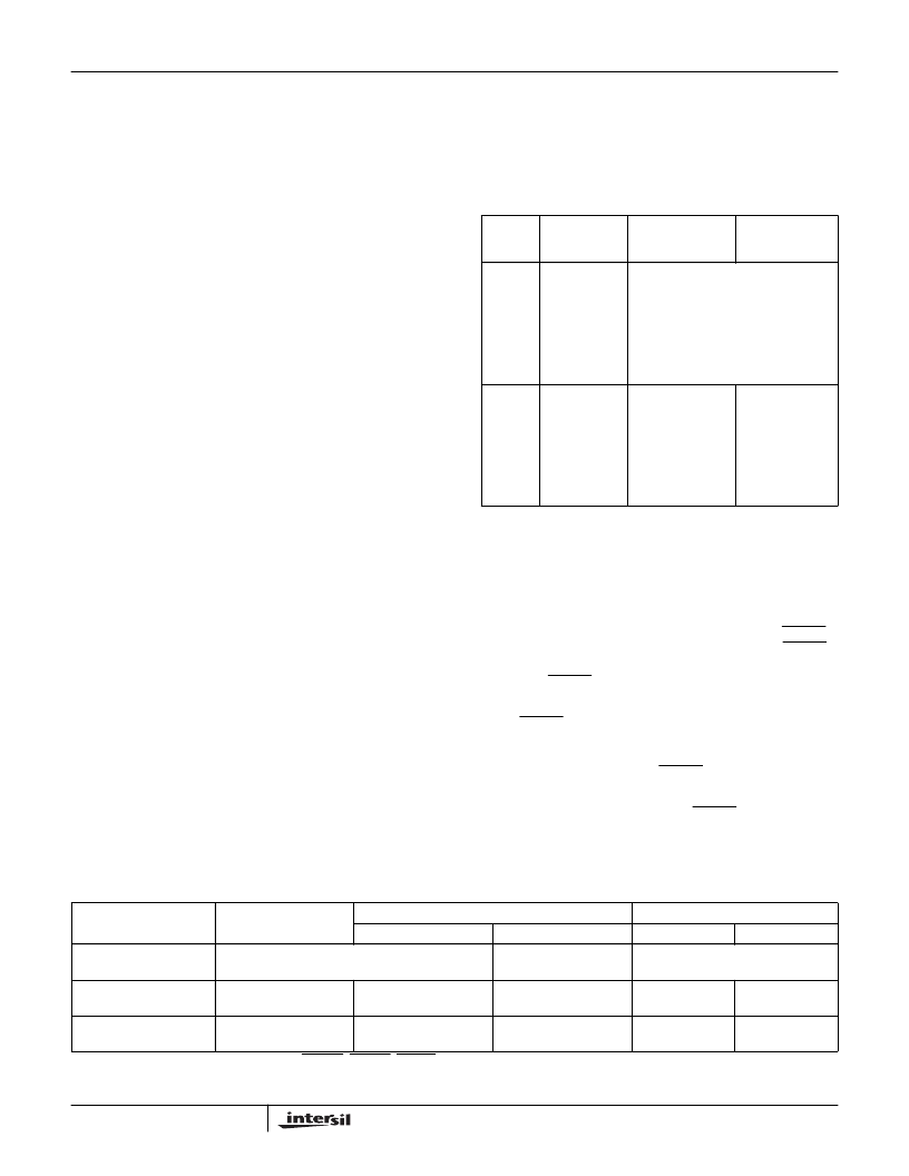
summarized in Table 2.
Figures 1, 2, and 3 show the timing of CLK, CLK2, BLANK,
and the pixel input data with respect to each other. BLANK
may be an input or an output; the figures show both. When it
is an input, BLANK must arrive coincident with the pixel input
data; all are sampled at the same time.
When BLANK is an output, its timing with respect to the pixel
inputs depends on the blank timing select bit in the
timing_I/O_1 register. If the bit is cleared, the
HMP8190/HMP8191 negates BLANK one CLK cycle before
it samples the pixel inputs.
If the bit is set, the encoder negates BLANK during the same
CLK cycle in which it samples the input data. In effect, the
input data must arrive one CLK cycle earlier than when the
bit is cleared. This mode is not shown in the figures.
TABLE 1. PIXEL DATA INPUT FORMATS
16-BIT
4:2:2
YCBCR
Cb0, Cr0
Cb1, Cr1
Cb2, Cr2
Cb3, Cr3
Cb4, Cr4
Cb5, Cr5
Cb6, Cr6
Cb7, Cr7
Y0
Y1
Y2
Y3
Y4
Y5
Y6
Y7
Y7, Cb7, Cr7
PIN
NAME
P0
P1
P2
P3
P4
P5
P6
P7
P8
P9
P10
P11
P12
P13
P14
P15
8-BIT
4:2:2
YCBCR
BT.656
Ignored
Y0, Cb0, Cr0
Y1, Cb1, Cr1
Y2, Cb2, Cr2
Y3, Cb3, Cr3
Y4, Cb4, Cr4
Y5, Cb5, Cr5
Y6, Cb6, Cr6
YCbCr Data,
SAV and EAV
Sequences,
and
Ancillary Data
TABLE 2. PIXEL INPUT AND CONTROL SIGNAL I/O TIMING
INPUT FORMAT
INPUT PIXEL DATA
SAMPLE
VIDEO TIMING CONTROL
(NOTE 1)
CLK FREQUENCY
INPUT SAMPLE
OUTPUT ON
INPUT
OUTPUT
16-Bit YCbCr
Rising edge of CLK2 when CLK is low
Rising edge of CLK2
when CLK is high.
One-half CLK2
8-Bit YCbCr
Every rising edge of
CLK2
Every rising edge of
CLK2
Any rising edge of CLK2
Ignored
One-half CLK2
BT.656
Every rising edge of
CLK2
Not Allowed
Any rising edge of CLK2
Ignored
One-half CLK2
NOTE: Video timing control signals include HSYNC, VSYNC, BLANK and FIELD. The sync and blanking I/O directions are independent; FIELD is
always an output.
HMP8190, HMP8191
相關(guān)PDF資料 |
PDF描述 |
|---|---|
| HMP8190CN | NTSC/PAL Video Encoder |
| HMP8190EVAL1 | NTSC/PAL Video Encoder |
| HMP8191 | NTSC/PAL Video Encoder |
| HMP8191CN | NTSC/PAL Video Encoder |
| HMPS650 | NPN SILICON TRANSISTOR |
相關(guān)代理商/技術(shù)參數(shù) |
參數(shù)描述 |
|---|---|
| HMP8190CN | 制造商:INTERSIL 制造商全稱(chēng):Intersil Corporation 功能描述:NTSC/PAL Video Encoder |
| HMP8190EVAL1 | 制造商:INTERSIL 制造商全稱(chēng):Intersil Corporation 功能描述:NTSC/PAL Video Encoder |
| HMP8191 | 制造商:INTERSIL 制造商全稱(chēng):Intersil Corporation 功能描述:NTSC/PAL Video Encoder |
| HMP8191CN | 制造商:INTERSIL 制造商全稱(chēng):Intersil Corporation 功能描述:NTSC/PAL Video Encoder |
| HMP8201CN | 制造商:未知廠家 制造商全稱(chēng):未知廠家 功能描述:Compression/Expansion Circuit |
發(fā)布緊急采購(gòu),3分鐘左右您將得到回復(fù)。