- 您現(xiàn)在的位置:買賣IC網(wǎng) > PDF目錄385382 > HIP6502 (Intersil Corporation) Multiple Linear Power Controller with ACPI Control Interface PDF資料下載
參數(shù)資料
| 型號(hào): | HIP6502 |
| 廠商: | Intersil Corporation |
| 元件分類: | 基準(zhǔn)電壓源/電流源 |
| 英文描述: | Multiple Linear Power Controller with ACPI Control Interface |
| 中文描述: | 多重線性電源控制器ACPI控制接口 |
| 文件頁數(shù): | 8/14頁 |
| 文件大小: | 147K |
| 代理商: | HIP6502 |

8
Not shown in these diagrams is the deglitching feature used
to protect against false sleep state tripping. Both S3 and S5
pins are protected against noise by a 2
μ
s filter (typically 1 -
4
μ
s). This feature is useful in noisy computer environments if
the control signals have to travel over significant distances.
Additionally, the S3 pin features a 200
μ
s delay in
transitioning to sleep states. Once the S3 pin goes low, an
internal timer is activated. At the end of the 200
μ
s interval, if
the S5 pin is low, the HIP6502 switches into S5 sleep state; if
the S5 pin is high, the HIP6502 goes into S3 sleep state.
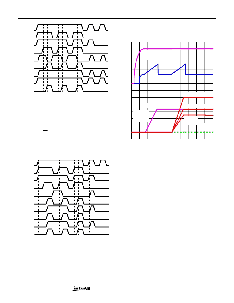
Soft-Start Circuit
SOFT-START INTO SLEEP STATES (S3, S4/S5)
The 5VSB POR function initiates the soft-start sequence. An
internal 10
μ
A current source charges an external capacitor.
The error amplifiers reference inputs are clamped to a level
proportional to the SS (soft-start) pin voltage. As the SS pin
voltage slews from about 1.25V to 2.5V, the input clamp
allows a rapid and controlled output voltage rise.
Figure 7 shows the soft-start sequence for the typical
application start-up in sleep state with all output voltages
enabled. At time T0 5VSB (bias) is applied to the circuit. At
time T1 the 5VSB surpasses POR level. An internal fast
charge circuit quickly raises the SS capacitor voltage to
approximately 1V, then the 10
μ
A current source continues
the charging. The soft-start capacitor voltage reaches
approximately 1.25V at time T2, at which point the
3.3V
DUAL
/3.3V
SB
error amplifier’s reference input starts its
transition, causing the output voltage to ramp up
proportionally. The ramp-up continues until time T3 when the
3.3V
DUAL
/3.3V
SB
voltage reaches the set value. After this
output reached its set value, as the soft-start capacitor
voltage reaches approximately 2.75V, the under-voltage
monitoring circuit of this output is activated and the soft-start
capacitor is quickly discharged to approximately 1.25V.
Following the 3ms (typical) time-out between T3 and T4, the
MSEL and EN5VDL selections are latched in, and the soft-
start capacitor commences a second ramp-up designed to
smoothly bring up the remainder of the voltages required by
the system. At time T5 all voltages are within regulation
limits, and as the SS voltage reaches 2.75V, all the
remaining UV monitors are activated and the SS capacitor is
quickly discharged to 1.25V, where it remains until the next
transition.
FIGURE 5. 5V
DUAL
TIMING DIAGRAM FOR EN5VDL = 0;
3V
DUAL
/3V
SB
5VSB
3.3V,
S3
S5
5VDLSB
DLA
3V3DLSB
3V3DL
5VDL
5V, 12V
FIGURE 6. 2.5V
MEM
, 3.3V
MEM
, AND 2.5V
CLK
TIMING
DIAGRAM; MSEL FLOATING (NOT CONNECTED)
5VSB
3.3V,
S3
S5
DRV2
VSEN1, 2
DEVICES
VSEN2
INTERNAL
VCLK
DLA
VSEN1
5V, 12V
FIGURE 7. SOFT-START INTERVAL IN A SLEEP STATE
(ALL OUTPUTS ENABLED)
0V
0V
TIME
SOFT-START
(1V/DIV)
OUTPUT
VOLTAGES
(1V/DIV)
V
OUT1
(3.3V
MEM
)
V
OUT2
(2.5V
MEM
)
V
OUT5
(5V
DUAL
)
T1 T2
T3
T0
5VSB
(1V/DIV)
T5
T4
V
OUT3
(3.3V
DUAL
/3.3V
SB
)
V
OUT4
(2.5V
CLK
)
HIP6502
相關(guān)PDF資料 |
PDF描述 |
|---|---|
| HIP6502CB | Multiple Linear Power Controller with ACPI Control Interface |
| HIP6503EVAL1 | Multiple Linear Power Controller with ACPI Control Interface |
| HIP6503CB | Circular Connector; No. of Contacts:37; Series:MS27467; Body Material:Aluminum; Connecting Termination:Crimp; Connector Shell Size:15; Circular Contact Gender:Socket; Circular Shell Style:Straight Plug; Insert Arrangement:15-35 |
| HIP6503 | Multiple Linear Power Controller with ACPI Control Interface(集成了多個(gè)線性電源控制器的芯片(ACPI控制接口)) |
| HIP6602ACB | FPGA 1600000 SYSTEM GATE 1.8 VOLT - NOT RECOMMENDED for NEW DESIGN |
相關(guān)代理商/技術(shù)參數(shù) |
參數(shù)描述 |
|---|---|
| HIP6502 WAF | 制造商:Intersil Corporation 功能描述: |
| HIP6502_00 | 制造商:INTERSIL 制造商全稱:Intersil Corporation 功能描述:Multiple Linear Power Controller with ACPI Control Interface |
| HIP6502B | 制造商:INTERSIL 制造商全稱:Intersil Corporation 功能描述:Multiple Linear Power Controller with ACPI Control Interface |
| HIP6502BCB | 制造商:Rochester Electronics LLC 功能描述:- Bulk |
| HIP6502BEVAL1 | 制造商:INTERSIL 制造商全稱:Intersil Corporation 功能描述:Multiple Linear Power Controller with ACPI Control Interface |
發(fā)布緊急采購,3分鐘左右您將得到回復(fù)。