- 您現(xiàn)在的位置:買賣IC網 > PDF目錄385382 > HIP6503 (Intersil Corporation) Multiple Linear Power Controller with ACPI Control Interface(集成了多個線性電源控制器的芯片(ACPI控制接口)) PDF資料下載
參數資料
| 型號: | HIP6503 |
| 廠商: | Intersil Corporation |
| 元件分類: | 基準電壓源/電流源 |
| 英文描述: | Multiple Linear Power Controller with ACPI Control Interface(集成了多個線性電源控制器的芯片(ACPI控制接口)) |
| 中文描述: | 多重線性電源控制器ACPI的控制接口(集成了多個線性電源控制器的芯片(ACPI的控制接口)) |
| 文件頁數: | 1/14頁 |
| 文件大?。?/td> | 152K |
| 代理商: | HIP6503 |

1
TM
File Number
4882.2
CAUTION: These devices are sensitive to electrostatic discharge; follow proper IC Handling Procedures.
1-888-INTERSIL or 321-724-7143
Intersil and Design is a trademark of Intersil Corporation.
Copyright Intersil Corporation 2000
HIP6503
Multiple Linear Power Controller with
ACPI Control Interface
The HIP6503 complements either an HIP6020 or an
HIP6021 in ACPI-compliant designs for microprocessor and
computer applications. The IC integrates four linear
controllers/regulators, switching, monitoring and control
functions into a 20 pin SOIC package. One linear controller
generates the 3.3V
DUAL
/3.3V
SB
voltage plane from the ATX
supply’s 5VSB output, powering the south bridge and the
PCI slots through an external pass transistor during sleep
states (S3, S4/S5). A second transistor is used to switch in
the ATX 3.3V output for operation during S0 and S1/S2
(active) operating states. A linear controllers/regulator
supplies at choice either of 2.5V or 3.3V memory power
through external pass transistors (switch for 3.3V setting) in
active states. During sleep states, integrated pass
transistors supply the sleep power. Another controller
powers up the 5V
DUAL
plane by switching in the ATX 5V
output in active states, and the ATX 5VSB in sleep states.
Two internal regulators output both a dedicated, noise-free
2.5V clock chip supply, as well as a 1.8V ICH2 resume well
voltage. The HIP6503’s operating mode (active outputs or
sleep outputs) is selectable through two digital control pins,
S3 and S5. Enabling sleep state support on the 5V
DUAL
output is offered through the EN5VDL pin. In active state, the
3.3V
DUAL
/3.3V
SB
and 2.5V
MEM
/3.3V
MEM
linear regulators
use external N-channel pass MOSFETs to connect the
outputs directly to the 3.3V input supplied by an ATX power
supply, for minimal losses. In sleep state, power delivery on
both outputs is transferred to NPN transistors - external to
the controller on the 3.3V
DUAL
/3.3V
SB
, internal on the
2.5V
MEM
/3.3V
MEM
. Active state regulation on the 2.5V
MEM
output is performed through an external NPN transistor. The
5V
DUAL
output is powered through two external MOS
transistors. In sleep states, a PMOS (or PNP) transistor
conducts the current from the ATX 5VSB output; while in
active state, current flow is transferred to an NMOS
transistor connected to the ATX 5V output. The operation of
the 5V
DUAL
output is dictated not only by the status of the
S3 and S5 pins, but that of the EN5VDL pin as well. The
3.3V
DUAL
/3.3V
SB
and 1.8V
SB
outputs are active for as long
as the ATX 5VSB voltage is applied to the chip. The 2.5V
CLK
output is only active during S0 and S1/S2, and uses the 3V3
pin as input source for its internal pass element.
Features
Provides 5 ACPI-Controlled Voltages
- 5V
DUAL
USB/Keyboard/Mouse (Active/Sleep)
- 3.3V
DUAL
/3.3V
SB
PCI/Auxiliary/LAN (Active/Sleep)
- 2.5V
MEM
RDRAM or 3.3V
MEM
SDRAM (Active/Sleep)
- 2.5V
CLK
Clock/Processor Terminations (Active Only)
- 1.8V
SB
ICH2 Resume
Excellent Output Voltage Regulation
- 3.3V
DUAL
/3.3V
SB
Output:
±
2.0% Over Temperature;
Sleep State Only
- 2.5V
MEM
/3.3V
MEM
Output:
±
2.0% Over Temperature;
Both Operational States (3.3V
MEM
in sleep only)
- 1.8V
SB
, 2.5V
CLK
Outputs:
±
2.0% Over Temperature
Small Size
- Very Low External Component Count
Dual Memory Voltage Selection Via FAULT/MSEL Pin
- 2.5V for RDRAM Memory
- 3.3V for SDRAM Memory
Undervoltage Monitoring of All Outputs with Centralized
FAULT Reporting and Temperature Shutdown
Applications
Motherboard Power Regulation for ACPI-Compliant
Computers
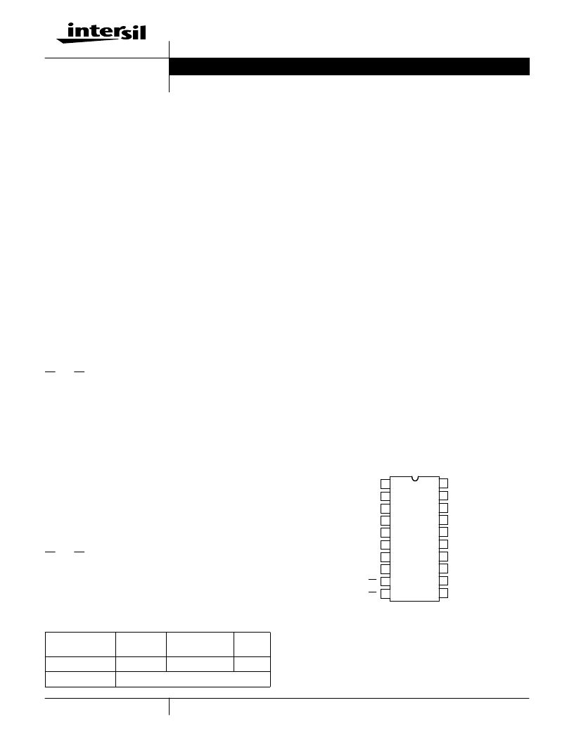
Pinout
HIP6503
(SOIC)
TOP VIEW
Ordering Information
PART NUMBER
TEMP.
RANGE (
o
C)
PACKAGE
PKG.
NO.
HIP6503CB
0 to 70
20 Ld SOIC
M20.3
HIP6503EVAL1
Evaluation Board
14
15
16
17
18
19
20
7
6
5
4
3
2
1
1V8IN
1V8SB
VCLK
3V3DLSB
3V3DL
5VSB
VSEN2
5V
5VDLSB
12V
DLA
SS
3V3
DRV2
EN5VDL
5VDL
13
8
11
12
10
9
S3
S5
FAULT/MSEL
GND
Data Sheet
November 2000
相關PDF資料 |
PDF描述 |
|---|---|
| HIP6602ACB | FPGA 1600000 SYSTEM GATE 1.8 VOLT - NOT RECOMMENDED for NEW DESIGN |
| HIP6602ACR | FPGA 1600000 SYSTEM GATE 1.8 VOLT - NOT RECOMMENDED for NEW DESIGN |
| HIP6602ACR-T | FPGA 1600000 SYSTEM GATE 1.8 VOLT - NOT RECOMMENDED for NEW DESIGN |
| HIP6602ACB-T | Dual Channel Synchronous Rectified Buck MOSFET Driver |
| HIRF840 | N-Channel Power MOSFET |
相關代理商/技術參數 |
參數描述 |
|---|---|
| HIP6503_05 | 制造商:INTERSIL 制造商全稱:Intersil Corporation 功能描述:Multiple Linear Power Controller with ACPI Control Interface |
| HIP6503CB | 制造商:Rochester Electronics LLC 功能描述:ACPI POWER MANAGEMENT CIRCUIT,20LD SOIC - Bulk 制造商:Intel 功能描述:9-CHANNEL POWER SUPPLY SUPPORT CKT, PDSO20 制造商:Intersil Corporation 功能描述:9-CHANNEL POWER SUPPLY SUPPORT CKT, PDSO20 |
| HIP6503CBZ | 功能描述:PMIC 解決方案 W/ANNEAL ACPI PWR MANAGEMNT CIRCUIT RoHS:否 制造商:Texas Instruments 安裝風格:SMD/SMT 封裝 / 箱體:QFN-24 封裝:Reel |
| HIP6503CBZ-T | 功能描述:PMIC 解決方案 W/ANNEAL ACPI PWR MG T CIRCUIT 20LD RoHS:否 制造商:Texas Instruments 安裝風格:SMD/SMT 封裝 / 箱體:QFN-24 封裝:Reel |
| HIP6503CR | 制造商:未知廠家 制造商全稱:未知廠家 功能描述:Analog IC |
發(fā)布緊急采購,3分鐘左右您將得到回復。