- 您現(xiàn)在的位置:買賣IC網(wǎng) > PDF目錄385382 > HIP6017BCB (INTERSIL CORP) FPGA - 100000 SYSTEM GATE 2.5 VOLT - NOT RECOMMENDED for NEW DESIGN PDF資料下載
參數(shù)資料
| 型號: | HIP6017BCB |
| 廠商: | INTERSIL CORP |
| 元件分類: | 穩(wěn)壓器 |
| 英文描述: | FPGA - 100000 SYSTEM GATE 2.5 VOLT - NOT RECOMMENDED for NEW DESIGN |
| 中文描述: | SWITCHING CONTROLLER, 215 kHz SWITCHING FREQ-MAX, PDSO28 |
| 封裝: | PLASTIC, MS-013AE, SOIC-28 |
| 文件頁數(shù): | 9/16頁 |
| 文件大?。?/td> | 139K |
| 代理商: | HIP6017BCB |

9
range, determine the R
OCSET
resistor from the equation
above with:
1. Themaximumr
DS(ON)
atthehighestjunctiontemperature.
2. The minimum I
OCSET
from the specification table.
3. Determine I
PEAK
for I
PEAK
> I
OUT(MAX)
+ (
I)/2,
where
I is the output inductor ripple current.
For an equation for the output inductor ripple current see the
section under component guidelines titled ‘Output Inductor
Selection’.
OUT1 Voltage Program
The output voltage of the PWM converter is programmed to
discrete levels between 1.3V
DC
and 3.5V
DC
. This output is
designed to supply the microprocessor core voltage. The voltage
identification (VID) pins program an internal voltage reference
(DACOUT) through a TTL-compatible 5-bit digital-to-analog
converter. The level of DACOUT also sets the PGOOD and OVP
thresholds.Table1specifiestheDACOUTvoltageforthedifferent
combinations of connections on the VID pins. The VID pins can
be left open for a logic 1 input, because they are internally pulled
upto+5Vbya10
μ
A(typically) current source.Changing theVID
inputs during operation is not recommended. The sudden
change in the resulting reference voltage could toggle the
PGOOD signal and exercise the over-voltage protection. The
‘11111’ VID pin combination resulting in an INHIBIT disables the
IC and the open-collector at the PGOOD pin.
Application Guidelines
Soft-Start Interval
Initially, the soft-start function clamps the error amplifier’s
output of the PWM converter. After the output voltage
increases to approximately 80% of the set value, the
reference input of the error amplifier is clamped to a voltage
proportional to the SS pin voltage. Both linear outputs follow
a similar start-up sequence. The resulting output voltage
sequence is shown in Figure 6.
The soft-start function controls the output voltage rate of rise
to limit the current surge at start-up. The soft-start interval is
programmed by the soft-start capacitor, C
SS
. Programming
a faster soft-start interval increases the peak surge current.
The peak surge current occurs during the initial output
voltage rise to 80% of the set value.
Shutdown
The PWM output does not switch until the soft-start voltage
(V
SS
) exceeds the oscillator’s valley voltage. Additionally, the
reference on each linear’s amplifier is clamped to the soft-
start voltage. Holding the SS pin low with an open drain or
collector signal turns off all three regulators.
The ‘11111’ VID code resulting in an INHIBIT as shown in
Table 1 also shuts down the IC.
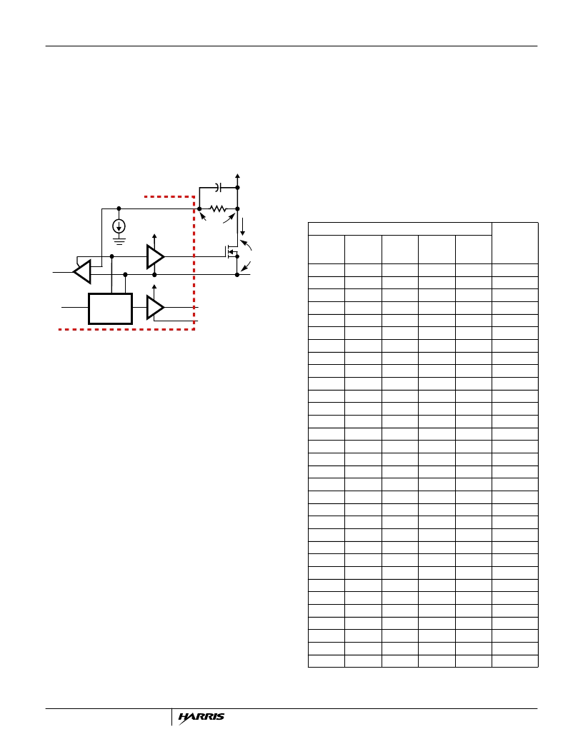
UGATE
OCSET
PHASE
OVER-
CURRENT1
+
-
GATE
CONTROL
VCC
OC1
200
μ
A
V
DS
i
D
V
SET
R
OCSET
V
IN
= +5V
OVER-CURRENT TRIP: V
DS
> V
SET
(i
D
x r
DS
(ON) > I
OCSET
x R
OCSET
)
I
OCSET
+
+
FIGURE 9. OVER-CURRENT DETECTION
PWM
V
PHASE
= V
IN
- V
DS
V
OCSET
= V
IN
- V
SET
DRIVE
HIP6017B
VCC
LGATE
PGND
TABLE 1. V
OUT1
VOLTAGE PROGRAM
PIN NAME
NOMINAL
OUT1
VOLTAGE
DACOUT
1.30
1.35
1.40
1.45
1.50
1.55
1.60
1.65
1.70
1.75
1.80
1.85
1.90
1.95
2.00
2.05
INHIBIT
2.1
2.2
2.3
2.4
2.5
2.6
2.7
2.8
2.9
3.0
3.1
3.2
3.3
3.4
3.5
VID4
0
0
0
0
0
0
0
0
0
0
0
0
0
0
0
0
1
1
1
1
1
1
1
1
1
1
1
1
1
1
1
1
VID3
1
1
1
1
1
1
1
1
0
0
0
0
0
0
0
0
1
1
1
1
1
1
1
1
0
0
0
0
0
0
0
0
VID2
1
1
1
1
0
0
0
0
1
1
1
1
0
0
0
0
1
1
1
1
0
0
0
0
1
1
1
1
0
0
0
0
VID1
1
1
0
0
1
1
0
0
1
1
0
0
1
1
0
0
1
1
0
0
1
1
0
0
1
1
0
0
1
1
0
0
VID0
1
0
1
0
1
0
1
0
1
0
1
0
1
0
1
0
1
0
1
0
1
0
1
0
1
0
1
0
1
0
1
0
NOTE: 0 = connected to GND or V
SS
, 1 = open or connected to 5V
through pull-up resistors.
HIP6017B
相關(guān)PDF資料 |
PDF描述 |
|---|---|
| HIP6018B | 100,000 System Gate FPGA - NOT RECOMMENDED for NEW DESIGN |
| HIP6018BCB | FPGA - 100000 SYSTEM GATE 2.5 VOLT - NOT RECOMMENDED for NEW DESIGN |
| HIP6019 | FPGA - 100000 SYSTEM GATE 2.5 VOLT - NOT RECOMMENDED for NEW DESIGN |
| HIP6019CB | Advanced Dual PWM and Dual Linear Power Control |
| HIP6019EVAL1 | Advanced Dual PWM and Dual Linear Power Control |
相關(guān)代理商/技術(shù)參數(shù) |
參數(shù)描述 |
|---|---|
| HIP6017BCB WAF | 制造商:Harris Corporation 功能描述: |
| HIP6017BCB-T | 制造商:Rochester Electronics LLC 功能描述:- Tape and Reel |
| HIP6017CB | 制造商:Rochester Electronics LLC 功能描述:- Bulk |
| HIP6017CB WAF | 制造商:Harris Corporation 功能描述: |
| HIP6017CB-T | 制造商:Rochester Electronics LLC 功能描述:- Bulk |
發(fā)布緊急采購,3分鐘左右您將得到回復(fù)。