- 您現(xiàn)在的位置:買賣IC網(wǎng) > PDF目錄385382 > HIP6017BCB (INTERSIL CORP) FPGA - 100000 SYSTEM GATE 2.5 VOLT - NOT RECOMMENDED for NEW DESIGN PDF資料下載
參數(shù)資料
| 型號: | HIP6017BCB |
| 廠商: | INTERSIL CORP |
| 元件分類: | 穩(wěn)壓器 |
| 英文描述: | FPGA - 100000 SYSTEM GATE 2.5 VOLT - NOT RECOMMENDED for NEW DESIGN |
| 中文描述: | SWITCHING CONTROLLER, 215 kHz SWITCHING FREQ-MAX, PDSO28 |
| 封裝: | PLASTIC, MS-013AE, SOIC-28 |
| 文件頁數(shù): | 12/16頁 |
| 文件大小: | 139K |
| 代理商: | HIP6017BCB |

12
High frequency decoupling capacitors should be placed as
close to the power pins of the load as physically possible. Be
careful not to add inductance in the circuit board wiring that
could cancel the usefulness of these low inductance
components. Consult with the manufacturer of the load on
specific decoupling requirements.
Use only specialized low-ESR capacitors intended for
switching regulator applications for the bulk capacitors. The
bulk capacitor’s ESR determines the output ripple voltage and
the initial voltage drop after a high slew-rate transient. An
aluminum electrolytic capacitor’s ESR value is related to the
case size with lower ESR available in larger case sizes.
However, the equivalent series inductance of these capacitors
increases with case size and can reduce the usefulness of the
capacitor to high slew-rate transient loading. Unfortunately,
ESL is not a specified parameter. Work with your capacitor
supplier and measure the capacitor’s impedance with
frequency to select suitable components. In most cases,
multiple electrolytic capacitors of small case size perform
better than a single large case capacitor. For a given transient
load magnitude, the output voltage transient response due to
the output capacitor characteristics can be approximated by
the following equation:
dI
Linear Output Capacitors
The output capacitors for the linear regulator and the linear
controller provide dynamic load current. The linear
controller uses dominant pole compensation integrated in
the error amplifier and is insensitive to output capacitor
selection. Capacitor, C
OUT3
should be selected for
transient load regulation.
The output capacitor for the linear regulator provides loop
stability. The linear regulator (OUT2) requires an output
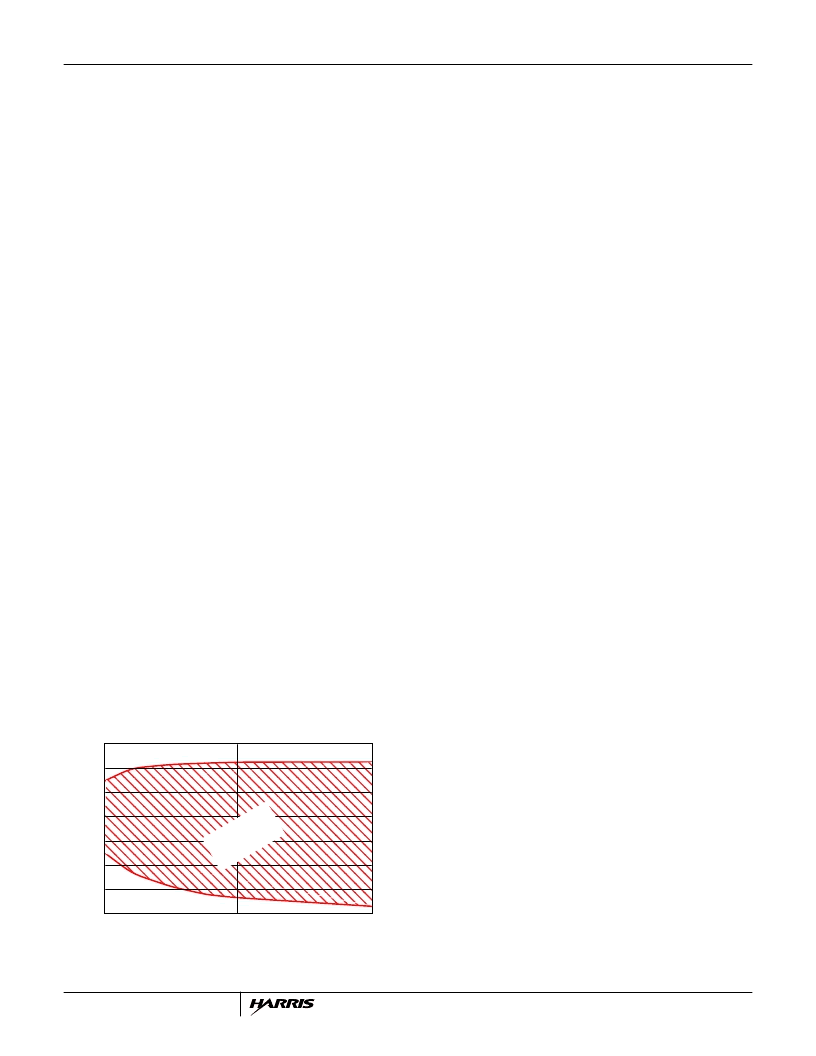
capacitor characteristic shown in Figure 13. The upper line
plots the 45 phase margin with 150mA load and the lower
line is the 45 phase margin limit with a 10mA load. Select a
C
OUT2
capacitor with characteristic between the two limits.
Output Inductor Selection
The PWM converter requires an output inductor. The output
inductor is selected to meet the output voltage ripple
requirements and sets the converter’s response time to a
load transient. The inductor value determines the converter’s
ripple current and the ripple voltage is a function of the ripple
current. The ripple voltage and current are approximated by
the following equations:
Increasing the value of inductance reduces the ripple current
and voltage. However, the large inductance values reduce
the converter’s response time to a load transient.
One of the parameters limiting the converter’s response to a
load transient is the time required to change the inductor
current. Given a sufficiently fast control loop design, the
HIP6017B will provide either 0% or 100% duty cycle in
response to a load transient. The response time is the time
interval required to slew the inductor current from an initial
current value to the post-transient current level. During this
interval the difference between the inductor current and the
transient current level must be supplied by the output
capacitors. Minimizing the response time can minimize the
output capacitance required.
The response time to a transient is different for the
application of load and the removal of load. The following
equations give the approximate response time interval for
application and removal of a transient load:
where: I
TRAN
is the transient load current step, t
RISE
is the
response time to the application of load, and t
FALL
is the
response time to the removal of load. With a +5V input
source, the worst case response time can be either at the
application or removal of load, and dependent upon the
output voltage setting. Be sure to check both of these
equations at the minimum and maximum output levels for the
worst case response time.
Input Capacitor Selection
The important parameters for the bulk input capacitor are the
voltage rating and the RMS current rating. For reliable
operation, select the bulk capacitor with voltage and current
ratings above the maximum input voltage and largest RMS
current required by the circuit. The capacitor voltage rating
should be at least 1.25 times greater than the maximum
input voltage and a voltage rating of 1.5 times is a
conservative guideline.
Use a mix of input bypass capacitors to control the voltage
overshoot across the MOSFETs. Use ceramic capacitance
for the high frequency decoupling and bulk capacitors to
V
TRAN
ESL
--------------------
×
ESR
I
TRAN
×
+
=
10
1000
100
0.1
0.2
0.3
0.4
0.5
0.6
0.7
CAPACITANCE (
μ
F)
E
)
FIGURE 13. C
OUT2
OUTPUT CAPACITOR
STABLE
I
V
-------------------------------
V
O
–
S
V
IN
---------------
×
=
V
OUT
I
ESR
×
=
t
RISE
L
IN
I
OUT
×
----------–
=
t
FALL
L
------------------------------
I
OUT
×
=
HIP6017B
相關PDF資料 |
PDF描述 |
|---|---|
| HIP6018B | 100,000 System Gate FPGA - NOT RECOMMENDED for NEW DESIGN |
| HIP6018BCB | FPGA - 100000 SYSTEM GATE 2.5 VOLT - NOT RECOMMENDED for NEW DESIGN |
| HIP6019 | FPGA - 100000 SYSTEM GATE 2.5 VOLT - NOT RECOMMENDED for NEW DESIGN |
| HIP6019CB | Advanced Dual PWM and Dual Linear Power Control |
| HIP6019EVAL1 | Advanced Dual PWM and Dual Linear Power Control |
相關代理商/技術參數(shù) |
參數(shù)描述 |
|---|---|
| HIP6017BCB WAF | 制造商:Harris Corporation 功能描述: |
| HIP6017BCB-T | 制造商:Rochester Electronics LLC 功能描述:- Tape and Reel |
| HIP6017CB | 制造商:Rochester Electronics LLC 功能描述:- Bulk |
| HIP6017CB WAF | 制造商:Harris Corporation 功能描述: |
| HIP6017CB-T | 制造商:Rochester Electronics LLC 功能描述:- Bulk |
發(fā)布緊急采購,3分鐘左右您將得到回復。