- 您現(xiàn)在的位置:買賣IC網(wǎng) > PDF目錄385379 > HI20206JCP (INTERSIL CORP) Triple 8-Bit, 35 MSPS, RGB, 3-Channel D/A Converter PDF資料下載
參數(shù)資料
| 型號: | HI20206JCP |
| 廠商: | INTERSIL CORP |
| 元件分類: | DAC |
| 英文描述: | Triple 8-Bit, 35 MSPS, RGB, 3-Channel D/A Converter |
| 中文描述: | PARALLEL, 8 BITS INPUT LOADING, 0.016 us SETTLING TIME, 8-BIT DAC, PDIP42 |
| 封裝: | PLASTIC, DIP-42 |
| 文件頁數(shù): | 5/13頁 |
| 文件大?。?/td> | 171K |
| 代理商: | HI20206JCP |
10-5
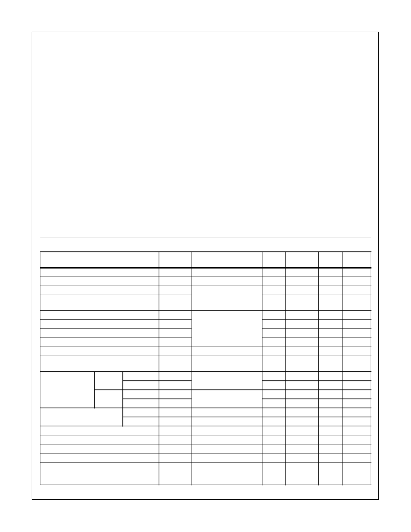
Absolute Maximum Ratings
Thermal Information
Supply Voltage (V
CC
). . . . . . . . . . . . . . . . . . . . . . . . . . . . . .0V to 7V
Input Voltage (Digital) (V
I
, V
CLK
) . . . . . . . . . . . . . . . . . -0.3V to V
CC
Output Voltage (Analog) (V
SET
). . . . . . . . . . . . . . V
CC
-2.1V to V
CC
Output Current
Analog (I
OUT
) . . . . . . . . . . . . . . . . . . . . . . . . . . . . . -3mA to 10mA
V
REF
Pin (I
REF
) . . . . . . . . . . . . . . . . . . . . . . . . . . . . -5mA to 0mA
Supply Voltage Range (Typ). . . . . . . . . . . . . . . . . . . . . . . 5V to 10V
Recommended Operating Conditions
Supply Voltage
AV
CC
, DV
CC
. . . . . . . . . . . . . . . . . . . . . . . . . . . . . . . .4.5V to 5.5V
AV
CC
-DV
CC
. . . . . . . . . . . . . . . . . . . . . . . . . . . . . . . -0.2V to 0.2V
AGND-DGND . . . . . . . . . . . . . . . . . . . . . . . . . . . . -0.05V to 0.05V
Digital Input Voltage
H Level (V
IH
, V
CLKH
) . . . . . . . . . . . . . . . . . . . . . . . .2.0V to DV
CC
L Level (V
IL
, V
CLKL
) . . . . . . . . . . . . . . . . . . . . . . . . DGND to 0.8V
V
SET
Input Voltage (V
SET
). . . . . . . . . . . . . . . . . . . . . . .0.7V to 0.9V
V
REF
Pin Current (I
REF
). . . . . . . . . . . . . . . . . . . . . .-3mA to -0.4mA
Clock Pulse Width
t
PW1
. . . . . . . . . . . . . . . . . . . . . . . . . . . . . . . . . . . . . . . . . . . .15ns
t
PW0
. . . . . . . . . . . . . . . . . . . . . . . . . . . . . . . . . . . . . . . . . . . .10ns
Temperature Range (T
OPR
) . . . . . . . . . . . . . . . . . . . . -40
o
C to 85
o
C
CAUTION: Stresses above those listed in “Absolute Maximum Ratings” may cause permanent damage to the device. This is a stress only rating and operation
of the device at these or any other conditions above those indicated in the operational sections of this specification is not implied.
Thermal Resistance (Typical, Note 2)
PDIP Package . . . . . . . . . . . . . . . . . . . . . . . . . . . . .
Maximum Storage Temperature Range (T
STG
) . . . .-65
o
C to 150
o
C
Maximum Lead Temperature (Soldering 10s). . . . . . . . . . . . . 300
o
C
θ
JA
(
o
C/W)
70
NOTE:
2.
θ
JA
is measured with the component mounted on an evaluation PC board in free air.
Electrical Specifications
T
A
= 25
o
C, AV
CC
= DV
CC
= 5V, AGND = DGND = 0V
PARAMETER
SYMBOL
TEST
CONDITIONS
MIN
TYP
MAX
UNITS
Resolution
RSL
-
8
-
Bit
Monotonic
MNT
-
Guarantee
-
-
Differential Linearity Error
DLE
V
SET
- AGND = 0.8V,
R
L
> 10k
-0.5
-
0.5
LSB
Integral Linearity Error
ILE
-0.4
-
0.4
% of Full
Scale
Maximum Conversion Speed
f
MAX
V
OFS
FSR
V
SET
- AGND = 0.8V,
R
L
> 10k
, C
L
< 20pF
35
-
-
MHz
Full Scale Output Voltage (Note 3)
0.85
1.0
1.15
V
P-P
%
RGB Output Voltage Full Scale Ratio (Note 4)
0
4
8
Output Zero Offset Voltage
V
OFFSET
R
O
I
D
-40
-6
0
mV
mA
Output Resistance
270
340
420
Dissipation Current
V
SET
- AGND = 0.8V,
R
L
> 10k
, I
REF
= -400
μ
A
V
I
= DV
CC
54
72
90
Digital Data Input
Current
H Level
Upper 2 Bits
I
IH(U)
I
IH(L)
I
IL(U)
I
IL(U)
I
CLKH
I
CLKL
I
SET
V
REF
t
S
t
H
CT
-
1.2
20
μ
A
μ
A
μ
A
μ
A
μ
A
μ
A
μ
A
V
Lower 6 Bits
-
0.6
10
L Level
Upper 2 Bits
V
I
= DGND
-10
0
10
Lower 6 Bits
-10
0
10
Clock Input Current
H Level
V
CLK
= DV
CC
V
CLK
= DGND
V
SET
- AGND = 0.8V
I
REF
= -400
μ
A
-
3
30
L Level
-10
0
10
V
SET
Input Current
Internal Reference Voltage
-5
-0.3
0
1.08
1.20
1.32
Set-Up Time
12
-
-
ns
Hold Time
3
-
-
ns
Crosstalk Among R, G and B
D/A OUT: 1V
P-P
, R
L
>10k
,
C
L
<20pF, f
DATA
= 7MHz,
f
CLK
= 14MHz, See Figure 5
-
-40
-33
dB
HI20206
相關(guān)PDF資料 |
PDF描述 |
|---|---|
| HI2559 | 1-Bit D/A Converter For Audio Application |
| HI2559JCQ | 1-Bit D/A Converter For Audio Application |
| HI2570 | 1-Bit AD/DA Converter For Audio Application |
| HI2570JCQ | 1-Bit AD/DA Converter For Audio Application |
| HI3-0506A-5Z | 16-Channel, 8-Channel, Differential 8-Channel and Differential 4-Channel, CMOS Analog MUXs with Active Overvoltage Protection |
相關(guān)代理商/技術(shù)參數(shù) |
參數(shù)描述 |
|---|---|
| HI2-0300/883 | 制造商:Rochester Electronics LLC 功能描述:10 CAN -55+125 15.0V DUAL SPST CMOS ANALOG SWITCH TTL INP - Bulk |
| HI2-0300-2 | 制造商:Rochester Electronics LLC 功能描述:- Bulk |
| HI2-0300-5 | 制造商:Rochester Electronics LLC 功能描述:- Bulk |
| HI2-0300-5 DIE | 制造商:Harris Corporation 功能描述: |
| HI2-0300-7 | 制造商:未知廠家 制造商全稱:未知廠家 功能描述:Interface IC |
發(fā)布緊急采購,3分鐘左右您將得到回復(fù)。