- 您現(xiàn)在的位置:買賣IC網(wǎng) > PDF目錄385375 > HFA1135IB96 (INTERSIL CORP) GT 3C 3#16S SKT RECP BOX PDF資料下載
參數(shù)資料
| 型號(hào): | HFA1135IB96 |
| 廠商: | INTERSIL CORP |
| 元件分類: | 音頻/視頻放大 |
| 英文描述: | GT 3C 3#16S SKT RECP BOX |
| 中文描述: | 1 CHANNEL, VIDEO PREAMPLIFIER, PDSO8 |
| 封裝: | PLASTIC, MS-012AA, SOIC-8 |
| 文件頁數(shù): | 4/15頁 |
| 文件大小: | 220K |
| 代理商: | HFA1135IB96 |

4
Application Information
Relevant Application Notes
The following Application Notes pertain to the HFA1135:
AN9653-Use and Application of Output Limiting
Amplifiers
AN9752-Sync Stripper and Sync Inserter for
Composite Video
AN9787-An Intuitive Approach to Understanding
Current Feedback Amplifiers
AN9420-Current Feedback Amplifier Theory and
Applications
AN9663-Converting from Voltage Feedback to Current
Feedback Amplifiers
These publications may be obtained from Intersil’s web site
(www.intersil.com) or via our AnswerFAX system.
Optimum Feedback Resistor
Although a current feedback amplifier’s bandwidth
dependency on closed loop gain isn’t as severe as that of a
voltage feedback amplifier, there can be an appreciable
decrease in bandwidth at higher gains. This decrease may
be minimized by taking advantage of the current feedback
amplifier’s unique relationship between bandwidth and R
F
.
All current feedback amplifiers require a feedback resistor,
even for unity gain applications, and R
F
, in conjunction with
the internal compensation capacitor, sets the dominant pole
of the frequency response. Thus, the amplifier’s bandwidth is
inversely proportional to R
F
. The HFA1135 design is
optimized for a 250
R
F
at a gain of +2. Decreasing R
F
decreases stability, resulting in excessive peaking and
overshoot (Note: Capacitive feedback will cause the same
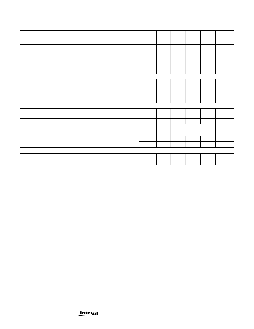
Slew Rate
(V
OUT
= 5V
P-P
, A
V
= -1, R
F
= 330
)
+SR
B
25
-
2300
-
V/
μ
s
V/
μ
s
-SR (Note 6)
B
25
-
1200
-
Settling Time
(V
OUT
= +2V to 0V step, Note 5)
To 0.1%
B
25
-
23
-
ns
To 0.05%
B
25
-
33
-
ns
To 0.02%
B
25
-
45
-
ns
VIDEO CHARACTERISTICS
A
V
= +2, R
F
= 250
,
Unless Otherwise Specified
R
L
= 150
R
L
= 75
R
L
= 150
R
L
= 75
A
V
= +2, R
F
= 250
,
V
H
= +1V, V
L
= -1V, Unless Otherwise Specified
V
IN
=
±
2V, A
V
= -1,
R
F
= 510
Overdrive Recovery Time (Note 5)
V
IN
=
±
1V
Negative Limit Range
Differential Gain (f = 3.58MHz)
B
25
-
0.02
-
%
B
25
-
0.03
-
%
Differential Phase (f = 3.58MHz)
B
25
-
0.04
-
Degrees
B
25
-
0.06
-
Degrees
OUTPUT LIMITING CHARACTERISTICS
Limit Accuracy (Note 5)
A
Full
-125
25
125
mV
B
25
-
0.8
-
ns
B
25
-5.0 to +2.5
V
Positive Limit Range
B
25
-2.5 to +5.0
V
Limit Input Bias Current
A
25
-
50
200
μ
A
μ
A
A
Full
-
80
200
POWER SUPPLY CHARACTERISTICS
Power Supply Range
C
25
±
4.5
-
±
5.5
V
Power Supply Current (Note 5)
A
Full
6.4
6.9
7.3
mA
NOTES:
2. Test Level: A. Production Tested; B. Typical or Guaranteed Limit Based on Characterization; C. Design Typical for Information Only.
3. The optimum feedback resistor for the HFA1135 at A
V
= +1 is 1.5k
. The Production Tested parameters are tested with R
F
= 510
because
the HFA1135 shares test hardware with the HFA1105 amplifier.
4. Undershoot dominates for output signal swings below GND (e.g., 0.5V
P-P
), yielding a higher overshoot limit compared to the V
OUT
= 0V to 0.5V
condition. See the “Application Information” section for details.
5. See Typical Performance Curves for more information.
6. Slew rates are asymmetrical if the output swings below GND (e.g., a bipolar signal). Positive unipolar output signals have symmetric positive and
negative slew rates comparable to the +SR specification. See the “Application Information” section, and the pulse response graphs for details.
Electrical Specifications
V
SUPPLY
=
±
5V, A
V
= +1, R
F
= 510
(Note 3), R
L
= 100
,
Unless Otherwise Specified
(Continued)
PARAMETER
TEST CONDITIONS
(NOTE 2)
TEST
LEVEL
TEMP.
(
o
C)
MIN
TYP
MAX
UNITS
HFA1135
相關(guān)PDF資料 |
PDF描述 |
|---|---|
| HFA1135IB | 360MHz, Low Power, Video Operational Amplifier with Output Limiting |
| HFA1135EVAL | 360MHz, Low Power, Video Operational Amplifier with Output Limiting |
| HFA1135 | 360MHz, Low Power, Video Operational Amplifier with Output Limiting(360MHz、低功耗視頻運(yùn)算放大器(帶輸出限制)) |
| HFA1205IP | 2.5V 144-mc CPLD - NOT RECOMMENDED for NEW DESIGN |
| HFA1205IB | Circular Connector; MIL SPEC:MIL-C-26482, Series I, Solder; Body Material:Aluminum; Series:PT06; No. of Contacts:55; Connector Shell Size:22; Connecting Termination:Solder; Circular Shell Style:Straight Plug |
相關(guān)代理商/技術(shù)參數(shù) |
參數(shù)描述 |
|---|---|
| HFA1135IBZ | 功能描述:視頻放大器 W/ANNEAL OPAMP 360MH ZCFBLIMIT8SOICIND RoHS:否 制造商:ON Semiconductor 通道數(shù)量:4 電源類型: 工作電源電壓:3.3 V, 5 V 電源電流: 最小工作溫度: 最大工作溫度: 封裝 / 箱體:TSSOP-14 封裝:Reel |
| HFA1135IBZ | 制造商:Intersil Corporation 功能描述:IC VIDEO OP AMP 360MHZ |
| HFA1135IBZ96 | 功能描述:視頻放大器 W/ANNEAL OPAMP 360MHZ CFB LIMIT IND RoHS:否 制造商:ON Semiconductor 通道數(shù)量:4 電源類型: 工作電源電壓:3.3 V, 5 V 電源電流: 最小工作溫度: 最大工作溫度: 封裝 / 箱體:TSSOP-14 封裝:Reel |
| HFA1135MJ/883 | 制造商:Rochester Electronics LLC 功能描述:- Bulk |
| HFA1135ML/883 | 制造商:Rochester Electronics LLC 功能描述:- Bulk |
發(fā)布緊急采購,3分鐘左右您將得到回復(fù)。