- 您現(xiàn)在的位置:買(mǎi)賣(mài)IC網(wǎng) > PDF目錄370423 > HAL300SO (MICRONAS SEMICONDUCTOR HOLDING AG) Differential Hall Effect Sensor IC PDF資料下載
參數(shù)資料
| 型號(hào): | HAL300SO |
| 廠商: | MICRONAS SEMICONDUCTOR HOLDING AG |
| 英文描述: | Differential Hall Effect Sensor IC |
| 中文描述: | 差分霍爾效應(yīng)傳感器IC |
| 文件頁(yè)數(shù): | 3/17頁(yè) |
| 文件大?。?/td> | 131K |
| 代理商: | HAL300SO |
第1頁(yè)第2頁(yè)當(dāng)前第3頁(yè)第4頁(yè)第5頁(yè)第6頁(yè)第7頁(yè)第8頁(yè)第9頁(yè)第10頁(yè)第11頁(yè)第12頁(yè)第13頁(yè)第14頁(yè)第15頁(yè)第16頁(yè)第17頁(yè)
HAL300
3
Micronas
Solderability
–
Package SOT-89A: according to IEC68-2-58
–
Package TO-92UA: according to IEC68-2-20
OUT
GND
3
2
1V
DD
Fig. 1:
Pin configuration
Functional Description
This Hall effect sensor is a monolithic integrated circuit
with 2 Hall plates 2.05 mm apart that switches in
response to differential magnetic fields. If magnetic
fields with flux lines at right angles to the sensitive areas
are applied to the sensor, the biased Hall plates force
Hall voltages proportional to these fields. The difference
of the Hall voltages is compared with the actual thresh-
old level in the comparator. The temperature-dependent
bias increases the supply voltage of the Hall plates and
adjusts the switching points to the decreasing induction
of magnets at higher temperatures. If the differential
magnetic field exceeds the threshold levels, the open
drain output switches to the appropriate state. The built-
in hysteresis eliminates oscillation and provides
switching behavior of the output without oscillation.
Magnetic offset caused by mechanical stress at the Hall
plates is compensated for by using the
“
switching offset
compensation technique
”
: An internal oscillator pro-
vides a two phase clock (see Fig. 3). The difference of
the Hall voltages is sampled at the end of the first phase.
At the end of the second phase, both sampled differen-
tial Hall voltages are averaged and compared with the
actual switching point. Subsequently, the open drain
output switches to the appropriate state. The amount of
time that elapses from crossing the magnetic switch lev-
el to the actual switching of the output can vary between
zero and 1/f
osc
.
Shunt protection devices clamp voltage peaks at the
Output-Pin and V
DD
-Pin together with external series
resistors. Reverse current is limited at the V
DD
-Pin by an
internal series resistor up to
–
15 V. No external reverse
protection diode is needed at the V
DD
-Pin for values
ranging from 0 V to
–
15 V.
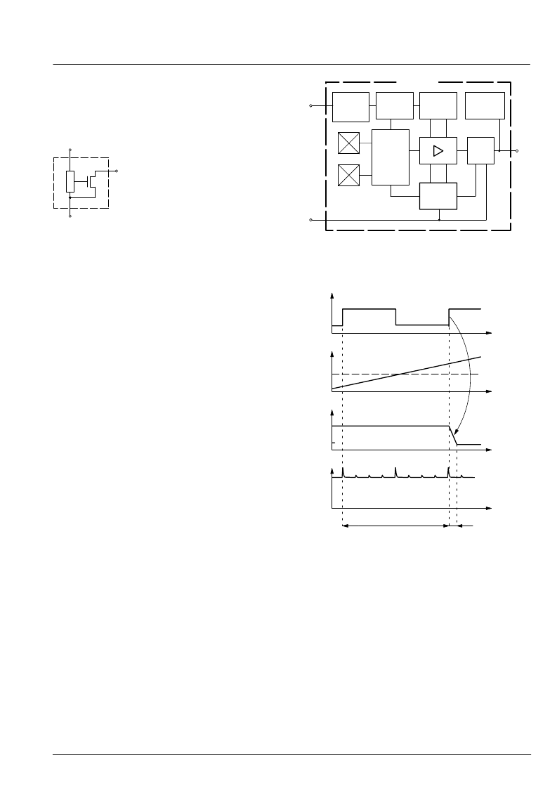
HAL300
Temperature
Dependent
Bias
Switch
Hysteresis
Control
Comparator
Output
V
DD
1
OUT
3
Clock
GND
2
Fig. 2:
HAL300 block diagram
Short Circuit &
Overvoltage
Protection
Reverse
Voltage &
Overvoltage
Protection
Hall Plate
S1
Hall Plate
S2
t
V
OL
V
OUT
V
OH
1/f
osc
= 16
μ
s
Fig. 3:
Timing diagram
B
B
ON
f
osc
t
t
t
f
t
I
DD
相關(guān)PDF資料 |
PDF描述 |
|---|---|
| HAL300 | Differential Hall Effect Sensor IC |
| HAL320 | Differential Hall Effect Sensor IC |
| HAL509 | Hall Effect Sensor Family |
| HAL502A | Hall Effect Sensor Family |
| HAL502E | 400 POS B2B® FEMALE CONNECTOR W/3M |
相關(guān)代理商/技術(shù)參數(shù) |
參數(shù)描述 |
|---|---|
| HAL300SO-A | 制造商:MICRONAS 制造商全稱(chēng):MICRONAS 功能描述:Differential Hall Effect Sensor IC |
| HAL300SO-C | 制造商:MICRONAS 制造商全稱(chēng):MICRONAS 功能描述:Differential Hall Effect Sensor IC |
| HAL300SO-E | 制造商:MICRONAS 制造商全稱(chēng):MICRONAS 功能描述:Differential Hall Effect Sensor IC |
| HAL300UA | 制造商:MICRONAS 制造商全稱(chēng):MICRONAS 功能描述:Differential Hall Effect Sensor IC |
| HAL300UA-A | 制造商:未知廠家 制造商全稱(chēng):未知廠家 功能描述:Hall-Effect Switch |
發(fā)布緊急采購(gòu),3分鐘左右您將得到回復(fù)。