- 您現(xiàn)在的位置:買賣IC網 > PDF目錄384385 > HA456CN (HARRIS SEMICONDUCTOR) 120MHz, Low Power, 8 x 8 Video Crosspoint Switch PDF資料下載
參數資料
| 型號: | HA456CN |
| 廠商: | HARRIS SEMICONDUCTOR |
| 元件分類: | 運動控制電子 |
| 英文描述: | 120MHz, Low Power, 8 x 8 Video Crosspoint Switch |
| 中文描述: | 8-CHANNEL, CROSS POINT SWITCH, PQFP44 |
| 文件頁數: | 1/15頁 |
| 文件大?。?/td> | 158K |
| 代理商: | HA456CN |
1
File Number
4153.2
CAUTION: These devices are sensitive to electrostatic discharge; follow proper IC Handling Procedures.
1-888-INTERSIL or 321-724-7143
|
Copyright
Intersil Corporation 1999
HA456
120MHz, Low Power, 8 x 8 Video
Crosspoint Switch
The HA456 is the first 8 x 8 video crosspoint switch suitable
for high performance video systems. Its high level of
integration significantly reduces component count, board
space, and cost. The crosspoint switch contains a digitally
controlled matrix of 64 fully buffered switches that connect
eight video input signals to any, or all, matrix outputs. Each
matrix output connects to an internal, high-speed (200V/
μ
s),
unity gain buffer capable of driving 400
and 5pF to
±
2V.
For applications requiring gain or increased drive capability,
the HA456 outputs can be connected directly to two
HFA1412 quad, gain of two video buffers, which are capable
of driving 75
loads.
This crosspoint’s true high impedance three-state output
capability, makes it feasible to parallel multiple HA456s and
form larger switch matrices.
Features
Fully Buffered Inputs and Outputs (A
V
= +1)
Routes Any Input Channel to Any Output Channel
Switches Standard and High Resolution Video Signals
Serial or Parallel Digital Interface
Expandable for Larger Switch Matrices
Wide Bandwidth . . . . . . . . . . . . . . . . . . . . . . . . . . 120MHz
High Slew Rate. . . . . . . . . . . . . . . . . . . . . . . . . . . 200V/
μ
s
Differential Gain and Phase . . . . . . .0.05%, 0.05 Degrees
Low Crosstalk at 10MHz . . . . . . . . . . . . . . . . . . . . . -55dB
Applications
Professional Video Switching and Routing
Security and Video Editing Systems
Ordering Information
PART NUMBER
TEMP.
RANGE (
o
C)
PACKAGE
PKG. NO.
HA456CN
0 to 70
44 Ld MQFP
Q44.10x10
HA456CM
0 to 70
44 Ld PLCC
N44.65
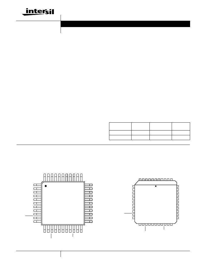
Pinouts
HA456 (MQFP)
TOP VIEW
HA456 (PLCC)
TOP VIEW
1
2
3
4
5
6
7
8
9
10
11
12 13 14 15 16 17
28
27
26
25
24
23
22
21
20
19
18
39 38 37 36 3534
33
32
31
30
29
44 43 42 41 40
I
A
A
D
D
N
V
O
D
O
D
A0
IN1
NC
IN2
DGND
NC
IN3
DGND
IN4
EDGE/LEVEL
IN5
OUT2
V-
OUT3
AGND
OUT4
NC
AGND
OUT5
AGND
OUT6
V+
V
I
S
I
V
N
W
L
C
C
O
44 43 42 41 40
39
38
37
36
35
34
33
32
31
30
29
28
27
1
2
3
4
5
6
26
25
24
23
22
21
20
19
18
7
8
9
10
11
12
13
14
15
16
17
A0
IN1
NC
IN2
DGND
NC
IN3
DGND
IN4
EDGE/LEVEL
IN5
I
A
A
D
D
N
V
O
D
O
D
V
I
S
I
V
N
W
L
C
C
O
OUT2
V-
OUT3
AGND
OUT4
NC
AGND
OUT5
AGND
OUT6
V+
Data Sheet
August 1999
相關PDF資料 |
PDF描述 |
|---|---|
| HA456 | 120MHz, Low Power, 8 x 8 Video Crosspoint Switch |
| HA4600CBZ | 480MHz, SOT-23, Video Buffer with Output Disable |
| HA4600CBZ96 | 480MHz, SOT-23, Video Buffer with Output Disable |
| HA4600CHZ96 | 480MHz, SOT-23, Video Buffer with Output Disable |
| HA4600CPZ | 480MHz, SOT-23, Video Buffer with Output Disable |
相關代理商/技術參數 |
參數描述 |
|---|---|
| HA456CP | 制造商:Rochester Electronics LLC 功能描述:- Bulk |
| HA456EVAL1 | 功能描述:交換機 IC 開發(fā)工具 EVAL PLATFORM HA456 RoHS:否 制造商:Maxim Integrated 產品:Evaluation Kits 類型:USB Power Switches 工具用于評估:MAX4984E 工作電源電壓:2.8 V to 5.5 V |
| HA457 | 制造商:INTERSIL 制造商全稱:Intersil Corporation 功能描述:95MHz, Low Power, AV = 2, 8 x 8 Video Crosspoint Switch |
| HA457CM | 制造商:Rochester Electronics LLC 功能描述:- Bulk |
| HA457CN | 制造商:Rochester Electronics LLC 功能描述:- Bulk |
發(fā)布緊急采購,3分鐘左右您將得到回復。