- 您現(xiàn)在的位置:買(mǎi)賣(mài)IC網(wǎng) > PDF目錄370212 > FMMT560A PDF資料下載
參數(shù)資料
| 型號(hào): | FMMT560A |
| 文件頁(yè)數(shù): | 10/247頁(yè) |
| 文件大?。?/td> | 2493K |
| 代理商: | FMMT560A |
第1頁(yè)第2頁(yè)第3頁(yè)第4頁(yè)第5頁(yè)第6頁(yè)第7頁(yè)第8頁(yè)第9頁(yè)當(dāng)前第10頁(yè)第11頁(yè)第12頁(yè)第13頁(yè)第14頁(yè)第15頁(yè)第16頁(yè)第17頁(yè)第18頁(yè)第19頁(yè)第20頁(yè)第21頁(yè)第22頁(yè)第23頁(yè)第24頁(yè)第25頁(yè)第26頁(yè)第27頁(yè)第28頁(yè)第29頁(yè)第30頁(yè)第31頁(yè)第32頁(yè)第33頁(yè)第34頁(yè)第35頁(yè)第36頁(yè)第37頁(yè)第38頁(yè)第39頁(yè)第40頁(yè)第41頁(yè)第42頁(yè)第43頁(yè)第44頁(yè)第45頁(yè)第46頁(yè)第47頁(yè)第48頁(yè)第49頁(yè)第50頁(yè)第51頁(yè)第52頁(yè)第53頁(yè)第54頁(yè)第55頁(yè)第56頁(yè)第57頁(yè)第58頁(yè)第59頁(yè)第60頁(yè)第61頁(yè)第62頁(yè)第63頁(yè)第64頁(yè)第65頁(yè)第66頁(yè)第67頁(yè)第68頁(yè)第69頁(yè)第70頁(yè)第71頁(yè)第72頁(yè)第73頁(yè)第74頁(yè)第75頁(yè)第76頁(yè)第77頁(yè)第78頁(yè)第79頁(yè)第80頁(yè)第81頁(yè)第82頁(yè)第83頁(yè)第84頁(yè)第85頁(yè)第86頁(yè)第87頁(yè)第88頁(yè)第89頁(yè)第90頁(yè)第91頁(yè)第92頁(yè)第93頁(yè)第94頁(yè)第95頁(yè)第96頁(yè)第97頁(yè)第98頁(yè)第99頁(yè)第100頁(yè)第101頁(yè)第102頁(yè)第103頁(yè)第104頁(yè)第105頁(yè)第106頁(yè)第107頁(yè)第108頁(yè)第109頁(yè)第110頁(yè)第111頁(yè)第112頁(yè)第113頁(yè)第114頁(yè)第115頁(yè)第116頁(yè)第117頁(yè)第118頁(yè)第119頁(yè)第120頁(yè)第121頁(yè)第122頁(yè)第123頁(yè)第124頁(yè)第125頁(yè)第126頁(yè)第127頁(yè)第128頁(yè)第129頁(yè)第130頁(yè)第131頁(yè)第132頁(yè)第133頁(yè)第134頁(yè)第135頁(yè)第136頁(yè)第137頁(yè)第138頁(yè)第139頁(yè)第140頁(yè)第141頁(yè)第142頁(yè)第143頁(yè)第144頁(yè)第145頁(yè)第146頁(yè)第147頁(yè)第148頁(yè)第149頁(yè)第150頁(yè)第151頁(yè)第152頁(yè)第153頁(yè)第154頁(yè)第155頁(yè)第156頁(yè)第157頁(yè)第158頁(yè)第159頁(yè)第160頁(yè)第161頁(yè)第162頁(yè)第163頁(yè)第164頁(yè)第165頁(yè)第166頁(yè)第167頁(yè)第168頁(yè)第169頁(yè)第170頁(yè)第171頁(yè)第172頁(yè)第173頁(yè)第174頁(yè)第175頁(yè)第176頁(yè)第177頁(yè)第178頁(yè)第179頁(yè)第180頁(yè)第181頁(yè)第182頁(yè)第183頁(yè)第184頁(yè)第185頁(yè)第186頁(yè)第187頁(yè)第188頁(yè)第189頁(yè)第190頁(yè)第191頁(yè)第192頁(yè)第193頁(yè)第194頁(yè)第195頁(yè)第196頁(yè)第197頁(yè)第198頁(yè)第199頁(yè)第200頁(yè)第201頁(yè)第202頁(yè)第203頁(yè)第204頁(yè)第205頁(yè)第206頁(yè)第207頁(yè)第208頁(yè)第209頁(yè)第210頁(yè)第211頁(yè)第212頁(yè)第213頁(yè)第214頁(yè)第215頁(yè)第216頁(yè)第217頁(yè)第218頁(yè)第219頁(yè)第220頁(yè)第221頁(yè)第222頁(yè)第223頁(yè)第224頁(yè)第225頁(yè)第226頁(yè)第227頁(yè)第228頁(yè)第229頁(yè)第230頁(yè)第231頁(yè)第232頁(yè)第233頁(yè)第234頁(yè)第235頁(yè)第236頁(yè)第237頁(yè)第238頁(yè)第239頁(yè)第240頁(yè)第241頁(yè)第242頁(yè)第243頁(yè)第244頁(yè)第245頁(yè)第246頁(yè)第247頁(yè)
8
www.fairchildsemi.com
FM24C256 rev. A.2
F
Write Protection
Programming of the memory array will not take place if the WP pin
is connected to V
CC
. The device will accept control and word
addresses; but if the memory accessed is write protected by the
WP pin, the FM24C256xxx will not generate an acknowledge after
the first byte of data has been received, and thus the program
cycle will not be started when the stop condition is asserted.
Read Operation
Read operations are initiated in the same manner as write
operations, with the exception that the R/W bit of the slave address
is set to "1". There are three basic read operations: current
address read, random read and sequential read.
CURRENT ADDRESS READ
Internally the FM24C256xxx contains an address counter that
maintains the address of the last word accessed, incremented by
one. Therefore, if the last access (either a read or write) was to
address n, the next read operation would access data from
address n+1. Upon receipt of the slave address with R/W set to
"1," the FM24C256xxx issues an acknowledge and transmits the
eight bit word. The master will not acknowledge the transfer but
does generate a stop condition, and therefore discontinues trans-
mission. Refer to Figure 7for the sequence of address, acknowl-
edge and data transfer.
RANDOM READ
Random read operations allow the master to access any memory
location in a random manner. Prior to issuing the slave address
with the R/W bit set to "1", the master must first perform a "dummy"
write operation. The master issues a start condition, a slave
address, and then the word address to be read. After the word
address acknowledge, the master immediately reissues the start
condition and the slave address with the R/W bit set to "1". This will
be followed by an acknowledge from the FM24C256xxx and then
by the eight bit word. The master will not acknowledge the transfer
but does generate the stop condition, and therefore the
FM24C256xxx discontinues transmission. Refer to Figure 8 for
the address, acknowledge, and data transfer sequence.
SEQUENTIAL READ
Sequential reads can be initiated as either a current address read
or random access read. The first word is transmitted in the same
manner as the other read modes; however, the master now
responds with an acknowledge, indicating it requires additional
data. The FM24C256xxx continues to output data for each ac-
knowledge received. The read operation is terminated by the
master not responding with an acknowledge or by generating a
stop condition.
The data output is sequential, with the data from address n,
followed by the data n+1. The address counter for read operations
increments all word address bits, allowing the entire memory
contents to be serially read during one operation. After the entire
memory has been read, the counter "rolls over" and the
FM24C256xxx continues to output data for each acknowledge
received. Refer to Figure 9for the address, acknowledge, and
data transfer sequence.
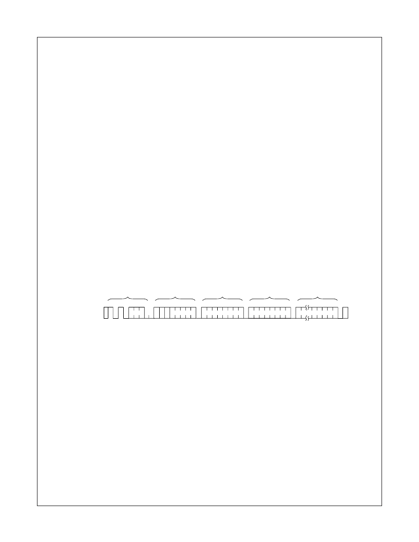
S
T
O
P
A
C
K
A
C
K
Bus Activity:
Master
SDA Line
1 0 1 0
0
Bus Activity
A
C
K
DATA n
DATA n+31
A
C
K
WORD
ADDRESS (1)
WORD
ADDRESS (0)
SLAVE
ADDRESS
S
T
A
R
T
DS800023-9
Page Write (Figure 6)
相關(guān)PDF資料 |
PDF描述 |
|---|---|
| FMMT92CSM | General Purpose PNP Transistor In a Hermetically Sealed Ceramic Surface Mount Package(通用PNP晶體管( 陶瓷表貼封裝)) |
| FMMT92CSM | GENERAL PURPOSE PNP TRANSISTOR IN A HERMETICALLY SEALED CERAMIC SURFACE MOUNT PACKAGE |
| FMN1.1 | TRANSISTOR | MOSFET | N-CHANNEL | 30V V(BR)DSS | CHIP |
| FMN1.2 | TRANSISTOR | MOSFET | N-CHANNEL | 33V V(BR)DSS | CHIP |
| FMN35.3 | TRANSISTOR | MOSFET | N-CHANNEL | 33V V(BR)DSS | CHIP |
相關(guān)代理商/技術(shù)參數(shù) |
參數(shù)描述 |
|---|---|
| FMMT560TA | 功能描述:兩極晶體管 - BJT PNP High V 500V RoHS:否 制造商:STMicroelectronics 配置: 晶體管極性:PNP 集電極—基極電壓 VCBO: 集電極—發(fā)射極最大電壓 VCEO:- 40 V 發(fā)射極 - 基極電壓 VEBO:- 6 V 集電極—射極飽和電壓: 最大直流電集電極電流: 增益帶寬產(chǎn)品fT: 直流集電極/Base Gain hfe Min:100 A 最大工作溫度: 安裝風(fēng)格:SMD/SMT 封裝 / 箱體:PowerFLAT 2 x 2 |
| FMMT560TC | 功能描述:兩極晶體管 - BJT PNP HighV 500V RoHS:否 制造商:STMicroelectronics 配置: 晶體管極性:PNP 集電極—基極電壓 VCBO: 集電極—發(fā)射極最大電壓 VCEO:- 40 V 發(fā)射極 - 基極電壓 VEBO:- 6 V 集電極—射極飽和電壓: 最大直流電集電極電流: 增益帶寬產(chǎn)品fT: 直流集電極/Base Gain hfe Min:100 A 最大工作溫度: 安裝風(fēng)格:SMD/SMT 封裝 / 箱體:PowerFLAT 2 x 2 |
| FMMT576 | 制造商:未知廠家 制造商全稱(chēng):未知廠家 功能描述: |
| FMMT589 | 制造商:Diodes Incorporated 功能描述:TRANSISTOR PNP SOT-23 |
| FMMT589 | 制造商:Diodes Incorporated 功能描述:TRANSISTOR PNP SOT-23 |
發(fā)布緊急采購(gòu),3分鐘左右您將得到回復(fù)。