- 您現(xiàn)在的位置:買賣IC網(wǎng) > PDF目錄375782 > FDS4953 (Microsemi Corporation) RES ARRAY 360 OHM 4TERM 2RES SMD PDF資料下載
參數(shù)資料
| 型號: | FDS4953 |
| 廠商: | Microsemi Corporation |
| 英文描述: | RES ARRAY 360 OHM 4TERM 2RES SMD |
| 中文描述: | 評估板 |
| 文件頁數(shù): | 11/18頁 |
| 文件大小: | 339K |
| 代理商: | FDS4953 |
LXE1710 E
VALUATION
B
OARD
MOSFET S
ELECTION
As seen in previous sections, the user can design the
output filter of the amplifier to meet performance or
costs targets. In addition, the amplifier’s power stage
(selection of MOSFETs) can be selected depending on
these tradeoffs. The efficiency of the amplifier circuit
can be approximated by the following equation.
P
+
(
Where
R
L
=
DC Resistance of Speaker
R
NDS
=
n-channel MOSFET on-resistance
U
SER
G
UIDE
Microsemi
Linfinity Microelectronics Division
11861 Western Avenue, Garden Grove, CA. 92841, 714-898-8121, Fax: 714-893-2570
Page 11
Copyright
2000
Rev. 1.1, 2000-12-01
CROSS
P
L
IND
PDS
NDS
L
IN
OUT
P
R
R
R
R
I
R
I
+
+
+
=
=
]
)
2
2
R
PDS
=
p-channel MOSFET on-resistance
R
IND
=
DC Resistance of Inductor
P
CROSS
=
MOSFET Switching Loss
The overall efficiency is a function of primarily the
MOSFETs and output filter inductors. The “Inductor”
section’s contribution will be considered later. The
MOSFET Power loss is a function of the on-resistance
and gate charge.
A
R
P
I
W
P
R
R
I
at
P
25
=
O
PDS
NDS
DS
5
4
25
Then
4
If
)]
(
Loss
Power
MOSFET
2
=
=
=
+
=
=
The LX1710 Evaluation Board is designed using
FDS4953
p-channel
and
MOSFETS.
FDS6612A
n-channel
W
P
R
R
DS
PDS
NDS
56
.
=
)]
095
.
03
.
)
095
.
,
03
.
2
+
=
=
=
MOSFET power loss is proportional to on-resistance.
n
S
f
CV
P
CROSS
2
Loss
Switching
MOSFET
=
=
Where
Assume
C
= Input Capacitance
V
= Supply Voltage
f
S
= Switching Frequency
n
= Number of MOSFETS
C
= 1000pF
V
= 15VDC
f
S
= 500kHz
W
P
CROSS
45
.
)
)(
10
500
)(
15
)(
10
1
3
2
9
=
×
×
=
MOSFET switching loss is proportional to total gate
charge, supply voltage, and switching frequency.
There are a few other important parameters to
consider when selecting the output power components
besides the on-resistance and gate charge of the
MOSFETs. The drain-source voltage must provide
ample margin for circuit noise and high speed
switching transients. Since the amplifier configuration
requires output bridge operation at the supply voltage,
the MOSFETs should have a drain-source voltage of
at least 50% greater than the supply voltage. The
power dissipation of the MOSFETs should also be
able to dissipate the heat generated by the internal
losses and be greater than the sum of P
DS
and P
CROSS
.
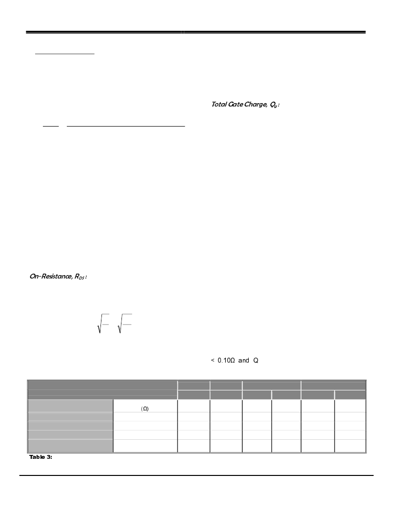
Linfinity recommends that in selecting MOSFETs, R
DS
0 1!1
2
several MOSFET options
.
g
<10nC. The table below provides
FDS6612A FDS4953
n-channel p-channel n-channel p-channel n-channel p-channel
Si4532ADY
IRF7105
Drain-Source On-Resistance
RDS(ON)@VGS = +/-10V
0.022
0.053
0.053
0.08
0.10
0.25
Drain-Source Voltage
Drain Current (continuous)
Total Gate Charge
VDSS (V)
30
-30
30
-30
25
-25
ID(continuous) (A)
8.4
-5
4.9
-3.9
3.5
-2.3
Q
g
(typical) (nC)
9
8
8
10
9.4
10
Manufacturer
Fairchild
Fairchild
Vishay
Siliconix
Vishay
Siliconix
International
Rectifier
International
Rectifier
MOSFET Component Options
相關(guān)PDF資料 |
PDF描述 |
|---|---|
| FDS6612A | EVALUATION KIT |
| FDS4953 | Dual P-Channel, Logic Level, PowerTrenchTM MOSFET |
| FDS6612A | Single N-Channel, Logic Level, PowerTrenchTM MOSFET |
| FDS5170N7 | 60V N-Channel PowerTrench MOSFET |
| FDS5670 | 60V N-Channel PowerTrench⑩ MOSFET |
相關(guān)代理商/技術(shù)參數(shù) |
參數(shù)描述 |
|---|---|
| FDS4953_02 | 制造商:FAIRCHILD 制造商全稱:Fairchild Semiconductor 功能描述:Dual 30V P-Channel PowerTrench MOSFET |
| FDS5170N7 | 功能描述:MOSFET 60V N-Ch PowerTrench RoHS:否 制造商:STMicroelectronics 晶體管極性:N-Channel 汲極/源極擊穿電壓:650 V 閘/源擊穿電壓:25 V 漏極連續(xù)電流:130 A 電阻汲極/源極 RDS(導(dǎo)通):0.014 Ohms 配置:Single 最大工作溫度: 安裝風(fēng)格:Through Hole 封裝 / 箱體:Max247 封裝:Tube |
| FDS5351 | 功能描述:MOSFET 60V N-Channel PowerTrench RoHS:否 制造商:STMicroelectronics 晶體管極性:N-Channel 汲極/源極擊穿電壓:650 V 閘/源擊穿電壓:25 V 漏極連續(xù)電流:130 A 電阻汲極/源極 RDS(導(dǎo)通):0.014 Ohms 配置:Single 最大工作溫度: 安裝風(fēng)格:Through Hole 封裝 / 箱體:Max247 封裝:Tube |
| FDS5670 | 功能描述:MOSFET SO-8 N-CH 60V RoHS:否 制造商:STMicroelectronics 晶體管極性:N-Channel 汲極/源極擊穿電壓:650 V 閘/源擊穿電壓:25 V 漏極連續(xù)電流:130 A 電阻汲極/源極 RDS(導(dǎo)通):0.014 Ohms 配置:Single 最大工作溫度: 安裝風(fēng)格:Through Hole 封裝 / 箱體:Max247 封裝:Tube |
| FDS5670 | 制造商:Fairchild Semiconductor Corporation 功能描述:MOSFET N SO-8 |
發(fā)布緊急采購,3分鐘左右您將得到回復(fù)。