- 您現(xiàn)在的位置:買賣IC網(wǎng) > PDF目錄375715 > FA5305APS (FUJI ELECTRIC HOLDINGS CO., LTD.) Bipolar IC For Switching Power Supply Control PDF資料下載
參數(shù)資料
| 型號(hào): | FA5305APS |
| 廠商: | FUJI ELECTRIC HOLDINGS CO., LTD. |
| 元件分類: | 基準(zhǔn)電壓源/電流源 |
| 英文描述: | Bipolar IC For Switching Power Supply Control |
| 中文描述: | 雙極集成電路開關(guān)電源控制 |
| 文件頁數(shù): | 7/17頁 |
| 文件大小: | 280K |
| 代理商: | FA5305APS |

7
FA5304AP(S)/FA5305AP(S)
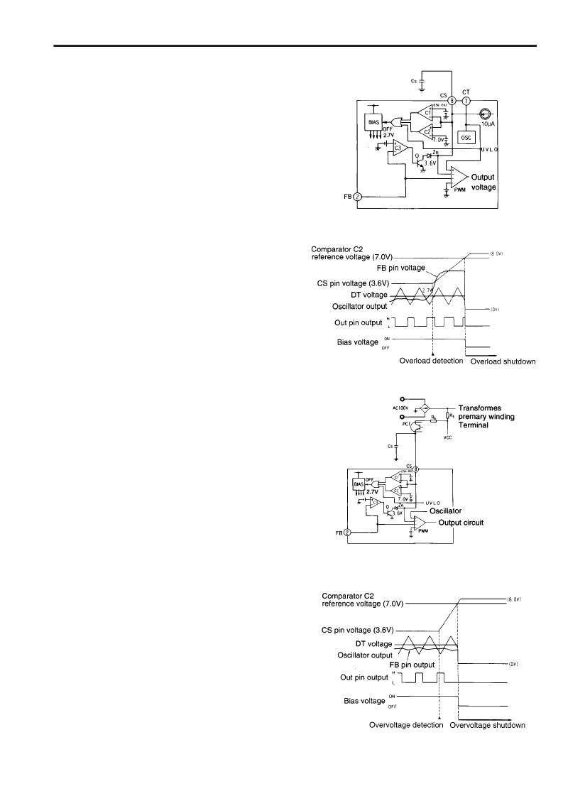
4.2 Overload shutdown
Figure 9 shows the overload shutdown circuit, and Figure 10 is
a timing chart which illustrates overload shutdown operation.If
the output voltage drops due to an overload or short-circuit, the
output voltage of the FB pin rises. If FB pin voltage exceeds
the reference voltage (2.7V) of comparator C3, the output of
comparator C3 switches low to turn transistor Q off. In normal
operation, transistor Q is on and the CS pin is clamped at 3.6V
by zener diode Zn. With Q off, the clamp is released and the
10
μ
A constant-current source begins to charge capacitor C
S
again and the CS pin voltage rises. When the CS pin voltage
exceeds the reference voltage (7.0V) of comparator C2, the
output of comparator C2 switches high to turn the bias circuit
off. The IC then enters the latched mode and shuts the output
down. Shutdown current consumption is 400
μ
A(V
CC
=9V).
This current must be supplied through the startup resistor. The
IC then discharges the MOSFET gates.
Shutdown operation initiated by an overload can be reset by
lowering supply voltage V
CC
below 8.7V or forcing the CS pin
voltage below 7.0V.The period t
OL
from the time that the output
is short-circuited to the time that the bias circuit turns off is
given by the following equation:
t
OL
(m
S
) = 340Cs(
μ
F).........................................(3)
4.3 Overvoltage shutdown
Figure 11 shows the overvoltage shutdown circuit, and Figure
12 is a timing chart which illustrates overvoltage shutdown
operation.
The optocoupler PC1 is connected between the CS and V
CC
pins. If the output voltage rises too high, the PC1 turns on to
raise the voltage at the CS pin via resistor R
6
. When the CS
pin voltage exceeds the reference voltage (7.0V) of
comparator C2, comparator C2 switches high to turn the bias
circuit off. The IC then enters the latched mode and shuts the
output down. The shutdown current consumption of the IC is
400
μ
A(V
CC
=9V). This current must be applied via startup
resistor R
5
.
The IC then discharges the MOSFET gates.
The shutdown operation initiated by an overvoltage condition
can be reset by lowering supply voltage V
CC
below 8.7V or
forcing the CS pin voltage below 7.0V.
During normal operation, the CS pin is clamped by a 3.6V
zener diode with a sink current of 150
μ
A max. Therefore, a
current of 150
μ
A or more must be supplied by the optocoupler
in order to raise the CS pin voltage above 7.0V.
Fig. 9 Overload shutdown circuit
Fig. 10 Overload shutdown timing chart
Fig. 11 Overvoltage shutdown circuit
Fig. 12 Overvoltage shutdown timing chart
相關(guān)PDF資料 |
PDF描述 |
|---|---|
| FA5314P | Bipolar IC For Switching Power Supply Control |
| FA5310 | CAPACITOR,SMD 603,100PF,50V,5% |
| FA5310BP | CAP 100PF 50V 5% C0G SMD-0603 BULK SN100 |
| FA5310BPS | CAP 100PF 50V 5% C0G SMD-0603 BULK SN100 |
| FA5311 | CAP 100PF 50V 5% C0G SMD-0603 TR-7-PA SN100 |
相關(guān)代理商/技術(shù)參數(shù) |
參數(shù)描述 |
|---|---|
| FA5305AS | 制造商:未知廠家 制造商全稱:未知廠家 功能描述:(367.00 k) |
| FA531 | 制造商:未知廠家 制造商全稱:未知廠家 功能描述:FA531硅NPN型超高頻大功率晶體管 |
| FA5310 | 制造商:FUJI 制造商全稱:Fuji Electric 功能描述:Bipolar IC For Switching Power Supply Control |
| FA5310BP | 制造商:FUJI 制造商全稱:Fuji Electric 功能描述:Bipolar IC For Switching Power Supply Control |
| FA5310BP(S) | 制造商:未知廠家 制造商全稱:未知廠家 功能描述: |
發(fā)布緊急采購,3分鐘左右您將得到回復(fù)。