- 您現(xiàn)在的位置:買賣IC網(wǎng) > PDF目錄375705 > F497 (Fujitsu Limited) 16-bit Proprietary Microcontroller CMOS PDF資料下載
參數(shù)資料
| 型號(hào): | F497 |
| 廠商: | Fujitsu Limited |
| 英文描述: | 16-bit Proprietary Microcontroller CMOS |
| 中文描述: | 16位微控制器專有的CMOS |
| 文件頁數(shù): | 38/40頁 |
| 文件大小: | 484K |
| 代理商: | F497 |
第1頁第2頁第3頁第4頁第5頁第6頁第7頁第8頁第9頁第10頁第11頁第12頁第13頁第14頁第15頁第16頁第17頁第18頁第19頁第20頁第21頁第22頁第23頁第24頁第25頁第26頁第27頁第28頁第29頁第30頁第31頁第32頁第33頁第34頁第35頁第36頁第37頁當(dāng)前第38頁第39頁第40頁
MB90495 Series
MB90495 Series Data Sheet (Advance Information)
38 / 40
FMG EMDC June 19, 2000
14.13 A/D Converter
(T
A
= –40 to +85
°
C, 3.0 V
≤
AVR – AVSS, V
CC
= AV
CC
= 5.0 V 10%, V
SS
= AV
SS
= 0 V)
*1: When not operating A/D converter, this is the current (V
CC
= AV
CC
= AVR = 5.0 V) when the CPU is stopped.
Terminology:
Conversion error :
Nonlinearlity :
Absolute maximum conversion deviation with respect to the theoretical conversion line.
Relative maximum conversion deviation with respect to the theoretical conversion line connecting to
the device-unique zero reading voltage and full-scale reading voltage.
Maximum conversion deviation in any two adjacent reading voltages with respect to the theoretical
LSB conversion step.
Input voltage which results in the minimum conversion value.
Input voltage which results in the maximum coversion value.
Differential non-linearlity :
Zero-reading voltage :
Full-scale reading voltage :
Notes:
1. The accuracy gets worse as AVR - AVSS becomes smaller.
2. Analog input external circuit output impedance should use the following conditions:
External circuit output impedance less than 15 k
3. If the external circuit output impedance is too high, there may be insufficient time for sampling of the analog voltage.
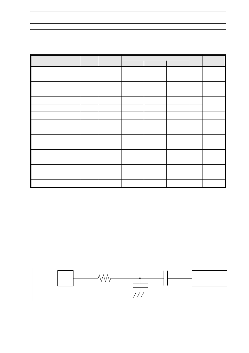
Figure 14.15 Analog Input pin
Parameter
Symbol
Pin
Rated Value
Units
Remarks
Min.
Typ.
Max.
Resolution
—
—
—
10
bit
Conversion error
—
—
—
—
5.0
LSB
Nonlinearity error
—
—
—
—
2.5
LSB
Differential nonlinearity error
—
—
—
—
1.9
LSB
Zero reading voltage
V
OT
AN0 to AN7
AVSS – 3.5
AVSS +0.5
AVSS + 4.5
LSB
1 LSB =
AVR/1024
Full scale reading voltage
V
FST
AN0 to AN7
AVR – 6.5
AVR –1.5
AVR + 1.5
LSB
Conversion time
—
—
—
176t
CP
—
ns
Sampling time
—
—
—
64t
CP
—
ns
Analog port input current
I
AIN
AN0 to AN7
—
—
10
μ
A
Analog input voltage range
V
AIN
AN0 to AN7
AVSS
—
AVR
V
Reference voltage range
—
AVR
AVSS + 2.7
—
AVCC
V
Power supply current
I
A
AVCC
—
5
—
mA
I
AH
AVCC
—
—
5
μ
A
*1
Reference voltage current
I
R
AVR
200
400
600
μ
A
I
RH
AVR
—
—
5
μ
A
*1
Offset between input channels
—
AN0 to AN7
—
—
4
LSB
C
1
C
0
Analog input
Converter
相關(guān)PDF資料 |
PDF描述 |
|---|---|
| F49L160BA | 16 Mbit (2M x 8/1M x 16) 3V Only CMOS Flash Memory |
| F49L160BA-70T | 16 Mbit (2M x 8/1M x 16) 3V Only CMOS Flash Memory |
| F49L160BA-90T | 16 Mbit (2M x 8/1M x 16) 3V Only CMOS Flash Memory |
| F49L160UA | 16 Mbit (2M x 8/1M x 16) 3V Only CMOS Flash Memory |
| F49L160UA-70T | 16 Mbit (2M x 8/1M x 16) 3V Only CMOS Flash Memory |
相關(guān)代理商/技術(shù)參數(shù) |
參數(shù)描述 |
|---|---|
| F-49700 | 制造商:LG Corporation 功能描述:WIRE & TERMINAL ASSY |
| F497500 | 制造商:FCI 功能描述: 制造商:Delphi Corporation 功能描述:2W_GEN3_FEM_CONN_BROWN_W |
| F-49757 | 制造商:LG Corporation 功能描述:KEYBOARD,10 KEY IR AND B |
| F49784-000 | 制造商:Elo Touch Solutions Inc 功能描述:ET1926L-7SWA-1 - Bulk |
| F-49824 | 制造商:LG Corporation 功能描述:CABINET AND |
發(fā)布緊急采購,3分鐘左右您將得到回復(fù)。