- 您現(xiàn)在的位置:買賣IC網(wǎng) > PDF目錄295887 > EP2C20F256I6N (ALTERA CORP) FPGA, 1196 CLBS, PBGA256 PDF資料下載
參數(shù)資料
| 型號: | EP2C20F256I6N |
| 廠商: | ALTERA CORP |
| 元件分類: | FPGA |
| 英文描述: | FPGA, 1196 CLBS, PBGA256 |
| 封裝: | LEAD FREE, FBGA-256 |
| 文件頁數(shù): | 83/168頁 |
| 文件大?。?/td> | 2206K |
| 代理商: | EP2C20F256I6N |
第1頁第2頁第3頁第4頁第5頁第6頁第7頁第8頁第9頁第10頁第11頁第12頁第13頁第14頁第15頁第16頁第17頁第18頁第19頁第20頁第21頁第22頁第23頁第24頁第25頁第26頁第27頁第28頁第29頁第30頁第31頁第32頁第33頁第34頁第35頁第36頁第37頁第38頁第39頁第40頁第41頁第42頁第43頁第44頁第45頁第46頁第47頁第48頁第49頁第50頁第51頁第52頁第53頁第54頁第55頁第56頁第57頁第58頁第59頁第60頁第61頁第62頁第63頁第64頁第65頁第66頁第67頁第68頁第69頁第70頁第71頁第72頁第73頁第74頁第75頁第76頁第77頁第78頁第79頁第80頁第81頁第82頁當前第83頁第84頁第85頁第86頁第87頁第88頁第89頁第90頁第91頁第92頁第93頁第94頁第95頁第96頁第97頁第98頁第99頁第100頁第101頁第102頁第103頁第104頁第105頁第106頁第107頁第108頁第109頁第110頁第111頁第112頁第113頁第114頁第115頁第116頁第117頁第118頁第119頁第120頁第121頁第122頁第123頁第124頁第125頁第126頁第127頁第128頁第129頁第130頁第131頁第132頁第133頁第134頁第135頁第136頁第137頁第138頁第139頁第140頁第141頁第142頁第143頁第144頁第145頁第146頁第147頁第148頁第149頁第150頁第151頁第152頁第153頁第154頁第155頁第156頁第157頁第158頁第159頁第160頁第161頁第162頁第163頁第164頁第165頁第166頁第167頁第168頁
Altera Corporation
2–9
February 2007
Cyclone II Device Handbook, Volume 1
Cyclone II Architecture
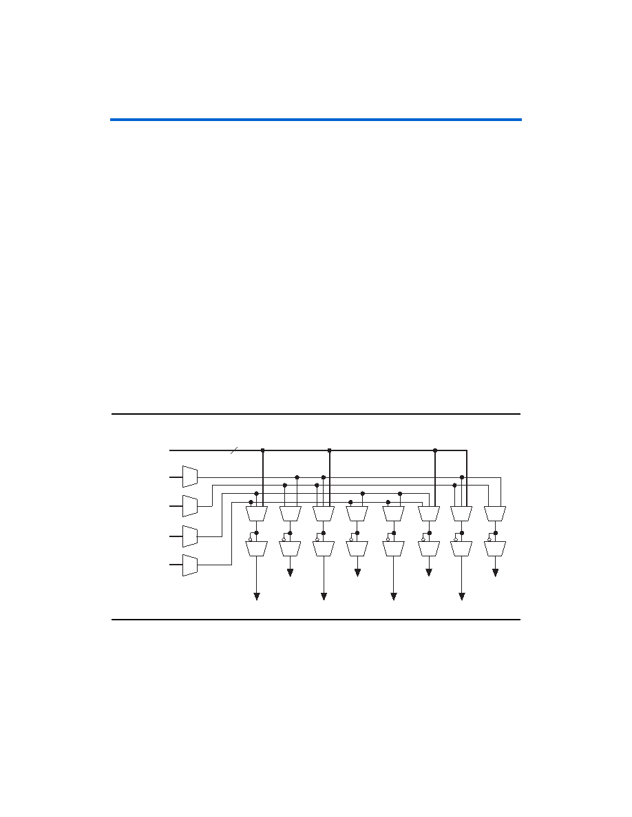
This gives a maximum of seven control signals at a time. When using the
LAB-wide synchronous load, the clkena of labclk1 is not available.
Additionally, register packing and synchronous load cannot be used
simultaneously.
Each LAB can have up to four non-global control signals. Additional LAB
control signals can be used as long as they are global signals.
Synchronous clear and load signals are useful for implementing counters
and other functions. The synchronous clear and synchronous load signals
are LAB-wide signals that affect all registers in the LAB.
Each LAB can use two clocks and two clock enable signals. Each LAB’s
clock and clock enable signals are linked. For example, any LE in a
particular LAB using the labclk1 signal also uses labclkena1. If the
LAB uses both the rising and falling edges of a clock, it also uses both
LAB-wide clock signals. De-asserting the clock enable signal turns off the
LAB-wide clock.
The LAB row clocks [5..0] and LAB local interconnect generate the LAB-
wide control signals. The MultiTrack interconnect’s inherent low skew
allows clock and control signal distribution in addition to data. Figure 2–7
shows the LAB control signal generation circuit.
Figure 2–7. LAB-Wide Control Signals
LAB-wide signals control the logic for the register’s clear signal. The LE
directly supports an asynchronous clear function. Each LAB supports up
to two asynchronous clear signals (
labclr1 and labclr2).
labclkena1
labclk2
labclk1
labclkena2
labclr1
Dedicated
LAB Row
Clocks
Local
Interconnect
Local
Interconnect
Local
Interconnect
Local
Interconnect
syncload
synclr
labclr2
6
相關(guān)PDF資料 |
PDF描述 |
|---|---|
| EP2SGX60CF780C3N | FPGA, 60440 CLBS, 717 MHz, PBGA780 |
| EP2SGX60CF780C3 | FPGA, 60440 CLBS, 717 MHz, PBGA780 |
| EP2SGX60CF780C4N | FPGA, 60440 CLBS, 717 MHz, PBGA780 |
| EP2SGX60CF780C4 | FPGA, 60440 CLBS, 717 MHz, PBGA780 |
| EP2SGX60CF780C5N | FPGA, 60440 CLBS, 640 MHz, PBGA780 |
相關(guān)代理商/技術(shù)參數(shù) |
參數(shù)描述 |
|---|---|
| EP2C20F256I8 | 功能描述:FPGA - 現(xiàn)場可編程門陣列 FPGA - Cyclone II 1172 LABs 152 IOs RoHS:否 制造商:Altera Corporation 系列:Cyclone V E 柵極數(shù)量: 邏輯塊數(shù)量:943 內(nèi)嵌式塊RAM - EBR:1956 kbit 輸入/輸出端數(shù)量:128 最大工作頻率:800 MHz 工作電源電壓:1.1 V 最大工作溫度:+ 70 C 安裝風格:SMD/SMT 封裝 / 箱體:FBGA-256 |
| EP2C20F256I8GA | 制造商:Altera Corporation 功能描述: |
| EP2C20F256I8N | 功能描述:FPGA - 現(xiàn)場可編程門陣列 FPGA - Cyclone II 1172 LABs 152 IOs RoHS:否 制造商:Altera Corporation 系列:Cyclone V E 柵極數(shù)量: 邏輯塊數(shù)量:943 內(nèi)嵌式塊RAM - EBR:1956 kbit 輸入/輸出端數(shù)量:128 最大工作頻率:800 MHz 工作電源電壓:1.1 V 最大工作溫度:+ 70 C 安裝風格:SMD/SMT 封裝 / 箱體:FBGA-256 |
| EP2C20F484C6 | 功能描述:FPGA - 現(xiàn)場可編程門陣列 FPGA - Cyclone II 1172 LABs 315 IOs RoHS:否 制造商:Altera Corporation 系列:Cyclone V E 柵極數(shù)量: 邏輯塊數(shù)量:943 內(nèi)嵌式塊RAM - EBR:1956 kbit 輸入/輸出端數(shù)量:128 最大工作頻率:800 MHz 工作電源電壓:1.1 V 最大工作溫度:+ 70 C 安裝風格:SMD/SMT 封裝 / 箱體:FBGA-256 |
| EP2C20F484C6N | 功能描述:FPGA - 現(xiàn)場可編程門陣列 FPGA - Cyclone II 1172 LABs 315 IOs RoHS:否 制造商:Altera Corporation 系列:Cyclone V E 柵極數(shù)量: 邏輯塊數(shù)量:943 內(nèi)嵌式塊RAM - EBR:1956 kbit 輸入/輸出端數(shù)量:128 最大工作頻率:800 MHz 工作電源電壓:1.1 V 最大工作溫度:+ 70 C 安裝風格:SMD/SMT 封裝 / 箱體:FBGA-256 |
發(fā)布緊急采購,3分鐘左右您將得到回復。