- 您現(xiàn)在的位置:買賣IC網(wǎng) > PDF目錄384281 > EDS2516APSA (Elpida Memory, Inc.) 256M bits SDRAM PDF資料下載
參數(shù)資料
| 型號: | EDS2516APSA |
| 廠商: | Elpida Memory, Inc. |
| 英文描述: | 256M bits SDRAM |
| 中文描述: | 256M比特內(nèi)存 |
| 文件頁數(shù): | 33/50頁 |
| 文件大小: | 703K |
| 代理商: | EDS2516APSA |
第1頁第2頁第3頁第4頁第5頁第6頁第7頁第8頁第9頁第10頁第11頁第12頁第13頁第14頁第15頁第16頁第17頁第18頁第19頁第20頁第21頁第22頁第23頁第24頁第25頁第26頁第27頁第28頁第29頁第30頁第31頁第32頁當前第33頁第34頁第35頁第36頁第37頁第38頁第39頁第40頁第41頁第42頁第43頁第44頁第45頁第46頁第47頁第48頁第49頁第50頁
EDS2516CDTA
Prelimimary Data Sheet E0545E40 (Ver. 4.0)
33
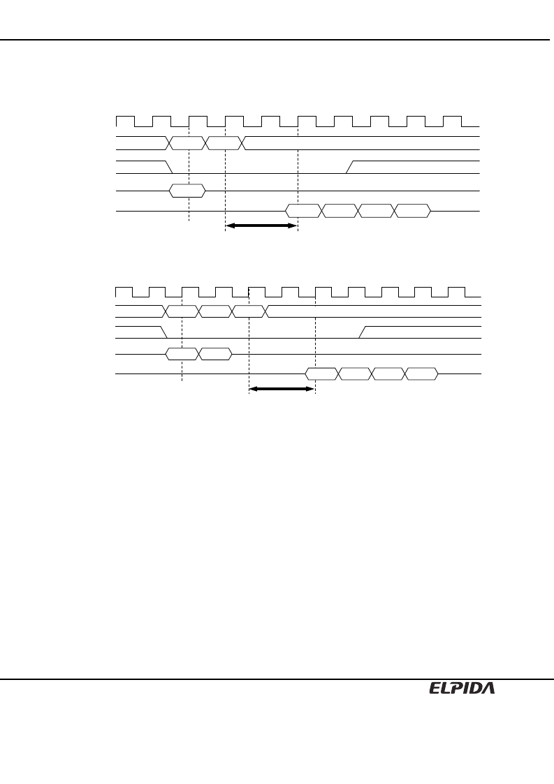
Write command to Read command interval:
1. Same bank, same ROW address: When the read command is executed at the same ROW address of the same
bank as the preceding write command, the read command can be performed after an interval of no less than 1
clock. However, in the case of a burst write, data will continue to be written until one clock before the read
command is executed.
CLK
Command
DQ (input)
WRIT
READ
in A0
out B1
out B2
out B3
out B0
DQ (output)
Column = A
Write
Column = B
Read
Column = B
Dout
/CAS Latency
UDQM
LDQM
Burst Write Mode
CL = 2
BL = 4
Bank 0
WRITE to READ Command Interval (1)
CLK
Command
DQ (input)
WRIT
READ
in A0
out B1
out B2
out B3
out B0
DQ (output)
Column = A
Write
Column = B
Read
Column = B
Dout
/CAS Latency
in A1
UDQM
LDQM
Burst Write Mode
CL = 2
BL = 4
Bank 0
WRITE to READ Command Interval (2)
2. Same bank, different ROW address: When the ROW address changes, consecutive read commands cannot be
executed; it is necessary to separate the two commands with a precharge command and a bank active
command.
3. Different bank: When the bank changes, the read command can be performed after an interval of no less than 1
clock, provided that the other bank is in the bank active state. However, in the case of a burst write, data will
continue to be written until one clock before the read command is executed (as in the case of the same bank and
the same address).
相關(guān)PDF資料 |
PDF描述 |
|---|---|
| EDS2516APSA-75 | 256M bits SDRAM |
| EDS2516APSA-75L | 256M bits SDRAM |
| EDS2516APSA-7A | 256M bits SDRAM |
| EDS2516APSA-7AL | 256M bits SDRAM |
| EDS2516APTA | 256M bits SDRAM |
相關(guān)代理商/技術(shù)參數(shù) |
參數(shù)描述 |
|---|---|
| EDS2516APSA-75 | 制造商:ELPIDA 制造商全稱:Elpida Memory 功能描述:256M bits SDRAM |
| EDS2516APSA-75L | 制造商:ELPIDA 制造商全稱:Elpida Memory 功能描述:256M bits SDRAM |
| EDS2516APSA-7A | 制造商:ELPIDA 制造商全稱:Elpida Memory 功能描述:256M bits SDRAM |
| EDS2516APSA-7AL | 制造商:ELPIDA 制造商全稱:Elpida Memory 功能描述:256M bits SDRAM |
| EDS2516APTA | 制造商:ELPIDA 制造商全稱:Elpida Memory 功能描述:256M bits SDRAM |
發(fā)布緊急采購,3分鐘左右您將得到回復。