- 您現(xiàn)在的位置:買賣IC網(wǎng) > PDF目錄384280 > EDE5104GBSA-4A-E (ELPIDA MEMORY INC) 512M bits DDR-II SDRAM PDF資料下載
參數(shù)資料
| 型號: | EDE5104GBSA-4A-E |
| 廠商: | ELPIDA MEMORY INC |
| 元件分類: | DRAM |
| 英文描述: | 512M bits DDR-II SDRAM |
| 中文描述: | 128M X 4 DDR DRAM, 0.6 ns, PBGA64 |
| 封裝: | MICRO, BGA-64 |
| 文件頁數(shù): | 32/66頁 |
| 文件大小: | 697K |
| 代理商: | EDE5104GBSA-4A-E |
第1頁第2頁第3頁第4頁第5頁第6頁第7頁第8頁第9頁第10頁第11頁第12頁第13頁第14頁第15頁第16頁第17頁第18頁第19頁第20頁第21頁第22頁第23頁第24頁第25頁第26頁第27頁第28頁第29頁第30頁第31頁當(dāng)前第32頁第33頁第34頁第35頁第36頁第37頁第38頁第39頁第40頁第41頁第42頁第43頁第44頁第45頁第46頁第47頁第48頁第49頁第50頁第51頁第52頁第53頁第54頁第55頁第56頁第57頁第58頁第59頁第60頁第61頁第62頁第63頁第64頁第65頁第66頁
EDE5104ABSE, EDE5108ABSE, EDE5116ABSE
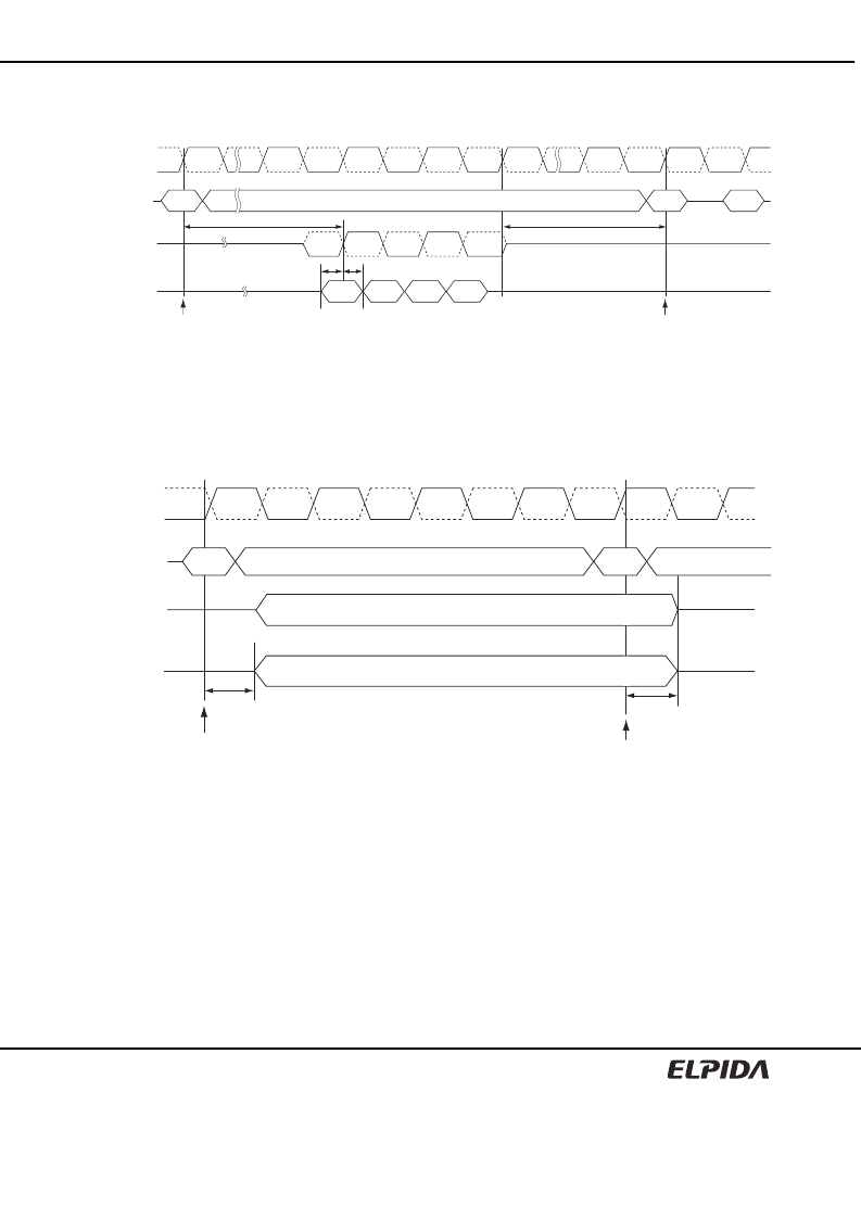
For proper operation of adjust mode, WL = RL
1 = AL + CL
1 clocks and tDS/tDH should be met as the Output
Impedance Control Register Set Cycle. For input data pattern for adjustment, DT0 to DT3 is a fixed order and not
affected by MRS addressing mode (i.e. sequential or interleave).
Data Sheet E0323E90 (Ver. 9.0)
32
Command
EMRS
OCD adjust mode
OCD calibration mode exit
NOP
DT0
tDS tDH
DT1
DT2
DT3
NOP
EMRS
CK
/CK
WL
tWR
DQS, /DQS
DQ_in
Output Impedance Control Register Set Cycle
Drive Mode
Drive mode, both drive (1) and drive (0), is used for controllers to measure DDR2 SDRAM Driver impedance before
OCD impedance adjustment. In this mode, all outputs are driven out tOIT after “Enter drive mode” command and all
output drivers are turned-off tOIT after “OCD calibration mode exit” command as the ”O(jiān)utput Impedance
Measurement/Verify Cycle”.
Command
Enter drivemode
OCD Calibration mode exit
NOP
CK
/CK
DQS, /DQS
High-Z
High-Z
DQs high for drive (1)
DQs low for drive (0)
tOIT
DQ
EMRS
EMRS
tOIT
DQs high and /DQS low for drive (1), DQs low and /DQS high for drive (0)
Output Impedance Measurement/Verify Cycle
相關(guān)PDF資料 |
PDF描述 |
|---|---|
| EDE5104AJSE | EDE5104AJSE |
| EDE5108AJBG | 512M bits DDR2 SDRAM |
| EDE5108AJBG-6E-E | 512M bits DDR2 SDRAM |
| EDE5108AJBG-8E-E | 512M bits DDR2 SDRAM |
| EDE5116AJBG | 512M bits DDR2 SDRAM |
相關(guān)代理商/技術(shù)參數(shù) |
參數(shù)描述 |
|---|---|
| EDE5104GBSA-5A-E | 制造商:ELPIDA 制造商全稱:Elpida Memory 功能描述:512M bits DDR-II SDRAM |
| EDE5108ABSE | 制造商:ELPIDA 制造商全稱:Elpida Memory 功能描述:512M bits DDR2 SDRAM |
| EDE5108ABSE-4A-E | 制造商:ELPIDA 制造商全稱:Elpida Memory 功能描述:512M bits DDR2 SDRAM |
| EDE5108ABSE-5C-E | 制造商:ELPIDA 制造商全稱:Elpida Memory 功能描述:512M bits DDR2 SDRAM |
| EDE5108ABSE-AE | 制造商:ELPIDA 制造商全稱:Elpida Memory 功能描述:512M bits DDR2 SDRAM for HYPER DIMM |
發(fā)布緊急采購,3分鐘左右您將得到回復(fù)。