- 您現在的位置:買賣IC網 > PDF目錄384280 > EDE5104AGSE-4A-E (ELPIDA MEMORY INC) Circular Connector; No. of Contacts:6; Series:MS27468; Body Material:Aluminum; Connecting Termination:Crimp; Connector Shell Size:9; Circular Contact Gender:Pin; Circular Shell Style:Jam Nut Receptacle; Insert Arrangement:9-35 RoHS Compliant: No PDF資料下載
參數資料
| 型號: | EDE5104AGSE-4A-E |
| 廠商: | ELPIDA MEMORY INC |
| 元件分類: | DRAM |
| 英文描述: | Circular Connector; No. of Contacts:6; Series:MS27468; Body Material:Aluminum; Connecting Termination:Crimp; Connector Shell Size:9; Circular Contact Gender:Pin; Circular Shell Style:Jam Nut Receptacle; Insert Arrangement:9-35 RoHS Compliant: No |
| 中文描述: | 128M X 4 DDR DRAM, 0.6 ns, PBGA60 |
| 封裝: | ROHS COMPLIANT, FBGA-60 |
| 文件頁數: | 43/66頁 |
| 文件大小: | 697K |
| 代理商: | EDE5104AGSE-4A-E |
第1頁第2頁第3頁第4頁第5頁第6頁第7頁第8頁第9頁第10頁第11頁第12頁第13頁第14頁第15頁第16頁第17頁第18頁第19頁第20頁第21頁第22頁第23頁第24頁第25頁第26頁第27頁第28頁第29頁第30頁第31頁第32頁第33頁第34頁第35頁第36頁第37頁第38頁第39頁第40頁第41頁第42頁當前第43頁第44頁第45頁第46頁第47頁第48頁第49頁第50頁第51頁第52頁第53頁第54頁第55頁第56頁第57頁第58頁第59頁第60頁第61頁第62頁第63頁第64頁第65頁第66頁
EDE5104ABSE, EDE5108ABSE, EDE5116ABSE
Data Sheet E0323E90 (Ver. 9.0)
43
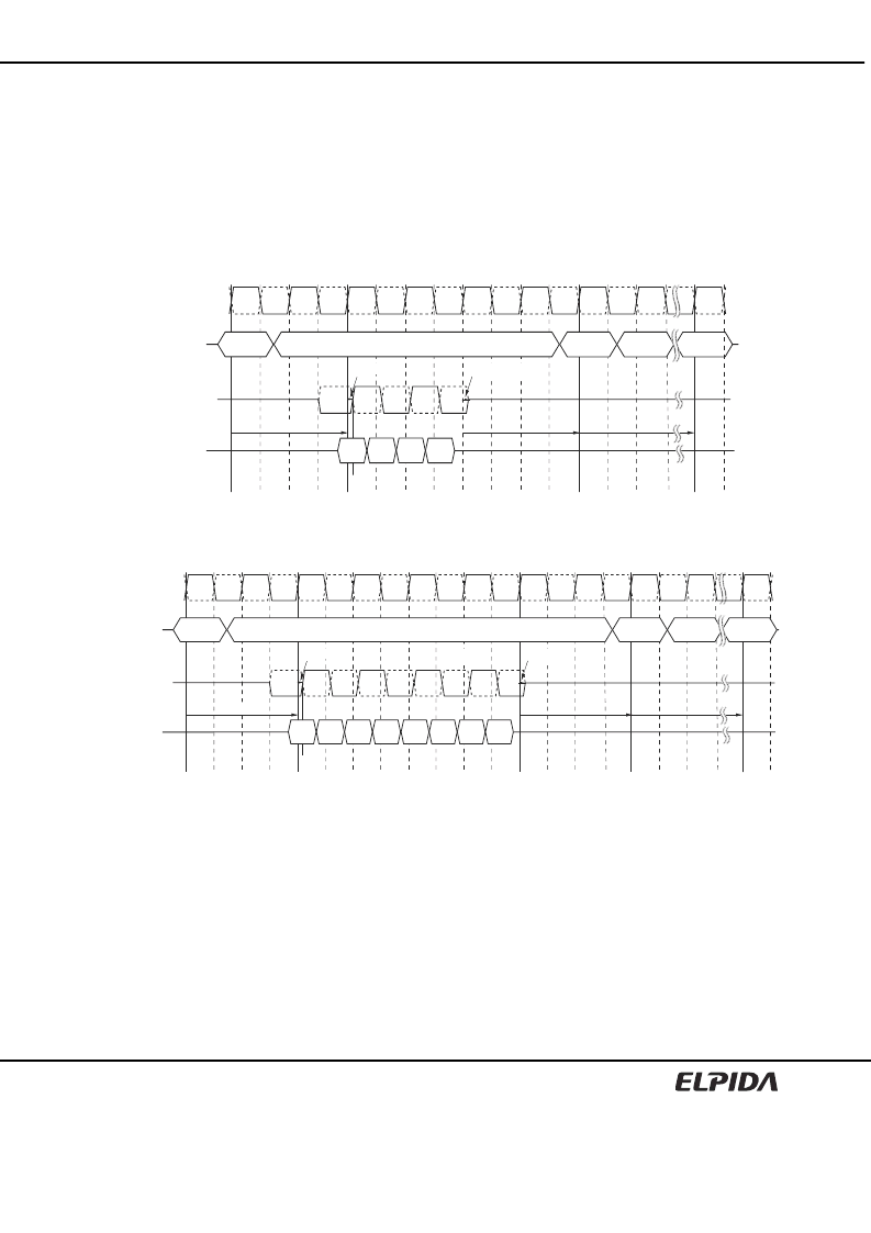
Burst Write Command [WRIT]
The Burst Write command is initiated by having /CS, /CAS and /WE low while holding /RAS high at the rising edge of
the clock. The address inputs determine the starting column address. Write latency (WL) is defined by a read
latency (RL) minus one and is equal to (AL + CL
1). A data strobe signal (DQS) should be driven low (preamble)
one clock prior to the WL. The first data bit of the burst cycle must be applied to the DQ pins at the first rising edge
of the DQS following the preamble. The tDQSS specification must be satisfied for write cycles. The subsequent
burst bit data are issued on successive edges of the DQS until the burst length of 4 is completed. When the burst
has finished, any additional data supplied to the DQ pins will be ignored. The DQ Signal is ignored after the burst
write operation is complete. The time from the completion of the burst write to bank precharge is the write recovery
time (tWR).
WRIT
NOP
CK
/CK
T0
T1
T2
T3
T4
T5
T6
T7
T9
Command
DQS, /DQS
DQ
>
tRP
=
>
tWR
=
in2
PRE
NOP
ACT
in1
in3
in0
=
Completion of
the Burst Write
<
tDQSS
WL = RL –1 = 2
Burst Write Operation (RL = 3, WL = 2, BL = 4 tWR = 2 (AL=0, CL=3))
WRIT
NOP
CK
/CK
T0
T1
T2
T3
T4
T5
T6
T7
T8
Command
DQS, /DQS
DQ
>
tRP
=
>
tWR
=
in2
in1
in3
in0
in6
in5
in7
in4
=
Completion of
the Burst Write
<
tDQSS
WL = RL –1 = 2
T9
T11
NOP
ACT
PRE
Burst Write Operation (RL = 3, WL = 2, BL = 8 (AL=0, CL=3))
相關PDF資料 |
PDF描述 |
|---|---|
| EDE5108AGSE-4A-E | Circular Connector; No. of Contacts:6; Series:MS27468; Body Material:Aluminum; Connecting Termination:Crimp; Connector Shell Size:9; Circular Contact Gender:Socket; Circular Shell Style:Jam Nut Receptacle; Insert Arrangement:9-35 RoHS Compliant: No |
| EDE5104AGSE-5C-E | Circular Connector; No. of Contacts:13; Series:MS27468; Body Material:Aluminum; Connecting Termination:Crimp; Connector Shell Size:11; Circular Contact Gender:Pin; Circular Shell Style:Jam Nut Receptacle; Insert Arrangement:11-35 RoHS Compliant: No |
| EDE5108AGSE-5C-E | 512M bits DDR2 SDRAM |
| EDE5104AGSE-6C-E | LJT 6C 6#20 SKT RECP |
| EDE5108AGSE-6C-E | LJT 13C 13#22M PIN RECP |
相關代理商/技術參數 |
參數描述 |
|---|---|
| EDE5104AGSE-5C-E | 制造商:ELPIDA 制造商全稱:Elpida Memory 功能描述:512M bits DDR2 SDRAM |
| EDE5104AGSE-6C-E | 制造商:ELPIDA 制造商全稱:Elpida Memory 功能描述:512M bits DDR2 SDRAM |
| EDE5104AGSE-6E-E | 制造商:ELPIDA 制造商全稱:Elpida Memory 功能描述:512M bits DDR2 SDRAM |
| EDE5104AHSE | 制造商:ELPIDA 制造商全稱:Elpida Memory 功能描述:512M bits DDR2 SDRAM |
| EDE5104AHSE-6E-E | 制造商:ELPIDA 制造商全稱:Elpida Memory 功能描述:512M bits DDR2 SDRAM |
發(fā)布緊急采購,3分鐘左右您將得到回復。