- 您現(xiàn)在的位置:買(mǎi)賣(mài)IC網(wǎng) > PDF目錄97873 > E6420-EDGE6420 Per-Pin Electronics Companion DAC PDF資料下載
參數(shù)資料
| 型號(hào): | E6420-EDGE6420 |
| 英文描述: | Per-Pin Electronics Companion DAC |
| 中文描述: | 按針腳電子伴侶援 |
| 文件頁(yè)數(shù): | 18/29頁(yè) |
| 文件大?。?/td> | 244K |
| 代理商: | E6420-EDGE6420 |
第1頁(yè)第2頁(yè)第3頁(yè)第4頁(yè)第5頁(yè)第6頁(yè)第7頁(yè)第8頁(yè)第9頁(yè)第10頁(yè)第11頁(yè)第12頁(yè)第13頁(yè)第14頁(yè)第15頁(yè)第16頁(yè)第17頁(yè)當(dāng)前第18頁(yè)第19頁(yè)第20頁(yè)第21頁(yè)第22頁(yè)第23頁(yè)第24頁(yè)第25頁(yè)第26頁(yè)第27頁(yè)第28頁(yè)第29頁(yè)
25
2000 Semtech Corp.
www .semtech.com
HIGH-PERFORMANCE PRODUCTS – ATE
Edge6420
AC Characteristics
r
e
t
e
m
a
r
a
Pl
o
b
m
y
Sn
i
Mp
y
Tx
a
Ms
t
i
n
U
s
t
u
p
n
I
l
a
t
i
g
i
D
)
1
e
t
o
N
(
s
e
m
i
T
p
U
t
e
S
K
C
g
n
i
s
i
R
o
t
I
D
S
4
2
K
C
g
n
i
s
i
R
o
t
)
e
g
d
e
g
n
i
s
i
r
(
E
C
4
2
K
C
g
n
i
s
i
R
o
t
)
e
g
d
e
g
n
i
s
i
r
(
E
T
A
D
P
U
)
3
,
2
s
e
t
o
N
(
T
I
D
S
_
U
S
T
E
C
_
U
S
T
D
P
U
_
U
S
0
1
0
1
5T
f
o
%
0
7
K
C
s
n
s
n
s
n
)
1
e
t
o
N
(
s
e
m
i
T
d
l
o
H
K
C
g
n
i
s
i
R
o
t
I
D
S
4
2
K
C
g
n
i
s
i
R
o
t
)
e
g
d
e
g
n
i
l
a
f
(
E
C
4
2
K
C
g
n
i
s
i
R
o
t
)
e
g
d
e
g
n
i
l
a
f
(
E
T
A
D
P
U
)
3
,
2
s
e
t
o
N
(
T
I
D
S
_
D
L
H
T
E
C
_
D
L
H
T
D
P
U
_
D
L
H
0
1
0
1
5T
f
o
%
0
7
K
C
s
n
s
n
s
n
K
C
)
5
,
1
s
e
t
o
N
(
V
0
3
.
±
V
3
.
3
=
D
V
D
t
a
x
a
m
F
)
5
e
t
o
N
(
e
l
c
y
C
y
t
u
D
%
0
5
o
t
0
3
e
l
c
y
C
y
t
u
D
%
0
7
F
x
a
m
3
0
2
z
H
M
z
H
M
)
5
,
4
s
e
t
o
N
(
0
5
.
±
V
0
.
5
=
D
V
D
t
a
x
a
m
F
e
l
c
y
C
y
t
u
D
%
0
5
o
t
0
3
e
l
c
y
C
y
t
u
D
%
0
7
F
x
a
m
5
3
z
H
M
z
H
M
)
1
e
t
o
N
(
e
l
c
y
C
y
t
u
DW
P
K
C
0
30
50
7%
h
t
d
i
W
e
s
l
u
P
T
E
S
E
RW
P
T
E
S
E
R
2s
)
1
e
t
o
N
(
e
m
i
T
g
n
i
l
t
e
S
e
g
a
t
l
o
V
t
u
p
t
u
O
K
C
m
o
r
f
(
)
E
T
A
D
P
U
o
t
g
n
i
d
n
o
p
s
e
r
o
c
)
R
S
F
%
5
2
0
.
0
o
t
(
V
0
1
,
p
e
t
S
e
l
a
c
S
l
u
F
D
,
B
,
A
s
p
u
o
r
G
r
o
f
F
n
0
1
:
d
a
o
L
F
n
0
1
:
d
a
o
L
s
T
0
3
0
5
2
0
7
0
7
s
s
)
R
S
F
%
5
2
0
.
0
o
t
(
V
7
1
,
p
e
t
S
e
l
a
c
S
l
u
F
C
p
u
o
r
G
r
o
f
F
n
0
1
:
d
a
o
L
F
n
0
1
:
d
a
o
L
0
5
0
1
4
.
0
5
1
s
s
m
e
m
i
T
g
n
i
l
t
e
S
t
n
e
r
u
C
t
u
p
t
u
O
)
%
5
2
0
.
o
t
(
E
p
u
o
r
G
F
n
1
:
d
a
o
L
F
n
0
1
:
d
a
o
L
3
5
0
3
2
0
1
0
5
s
s
)
%
8
.
o
t
(
F
p
u
o
r
G
F
n
1
:
d
a
o
L
F
n
0
1
:
d
a
o
L
4
.
4
9
2
0
1
0
5
s
s
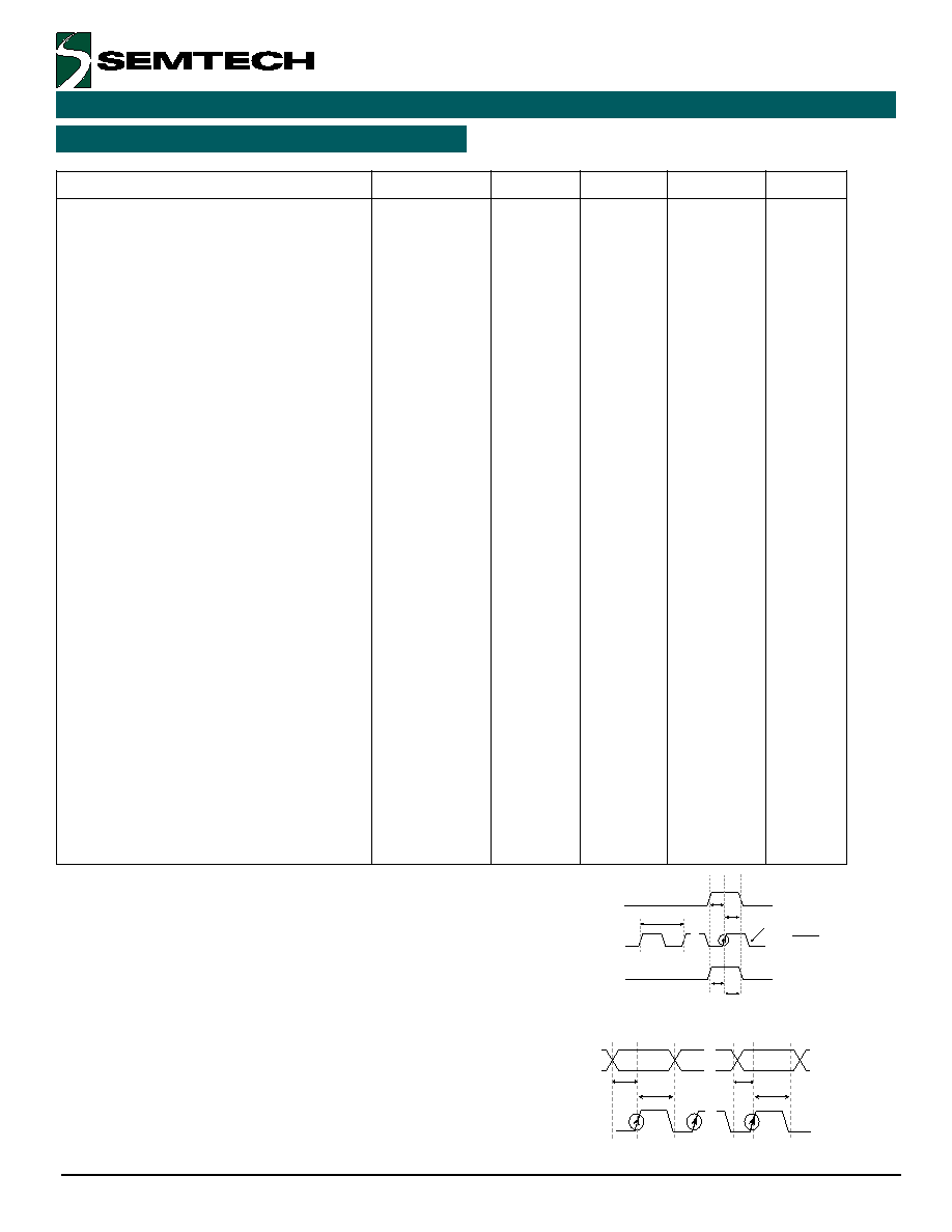
Figure 8. Shift Register Loading Timing Diagram
Figure 9. Central and Individual DAC Updating
Test conditions (unless otherwise specified): "Recommended Operating
Conditions".
Note 1:
Not production tested. Guaranteed by design and
characterization.
Note 2:
The max spec of 70% of TCK is not production tested.
Note 3:
CK24 refers to 24th rising clock edge, which corresponds
to a full shift register. Note that a falling CK24 edge is also
required for proper operation of circuit.
Note 4:
The 6420 is production tested at 55 MHz only, with 50%
duty cycle.
Note 5:
Duty cycle % shown refers to “high” duration of clock
in a period.
SDI
CK
CK1
CK24
Valid Data
A0
Valid Data
D15
TSU_SDI
THLD_SDI
CE
CK
UPDATE
CK24
CK1
THLD_CE
TSU_CE
TCK
THLD_UPDATE
TSU_UPDATE
Note: A 24th falling
CK edge is required for
DAC updating!
相關(guān)PDF資料 |
PDF描述 |
|---|---|
| E646-EDGE646 | Pin Electronics Driver. Window Comparator. and Switch Matrix |
| E647-EDGE647 | Pin Electronics Driver. Window Comparator. and Switch Matrix |
| E649-EDGE649 | Octal Pin Electronics Driver / Receiver |
| E670-EDGE670 | 500 MHz Window Comparator |
| E672-EDGE672 | 500 MHz Pin Electronics Window Comparator and Load |
相關(guān)代理商/技術(shù)參數(shù) |
參數(shù)描述 |
|---|---|
| E642123BIN WAF | 制造商:Texas Instruments 功能描述: |
| E642325A1N WAF | 制造商:Texas Instruments 功能描述: |
| E642332 | 制造商:Elo Touch Solutions Inc 功能描述:1919L, 18.5-INCH LCD, ACCUTOUCH, DUAL SERIAL/USB CONTROLLER, - Bulk |
| E642633 WAF | 制造商:Texas Instruments 功能描述: |
| E642919 WAF | 制造商:Texas Instruments 功能描述: |
發(fā)布緊急采購(gòu),3分鐘左右您將得到回復(fù)。