- 您現(xiàn)在的位置:買賣IC網(wǎng) > PDF目錄377001 > DSP56F826BU80E (飛思卡爾半導(dǎo)體(中國(guó))有限公司) 16-bit Digital Signal Controllers PDF資料下載
參數(shù)資料
| 型號(hào): | DSP56F826BU80E |
| 廠商: | 飛思卡爾半導(dǎo)體(中國(guó))有限公司 |
| 英文描述: | 16-bit Digital Signal Controllers |
| 中文描述: | 16位數(shù)字信號(hào)控制器 |
| 文件頁(yè)數(shù): | 13/56頁(yè) |
| 文件大小: | 700K |
| 代理商: | DSP56F826BU80E |
第1頁(yè)第2頁(yè)第3頁(yè)第4頁(yè)第5頁(yè)第6頁(yè)第7頁(yè)第8頁(yè)第9頁(yè)第10頁(yè)第11頁(yè)第12頁(yè)當(dāng)前第13頁(yè)第14頁(yè)第15頁(yè)第16頁(yè)第17頁(yè)第18頁(yè)第19頁(yè)第20頁(yè)第21頁(yè)第22頁(yè)第23頁(yè)第24頁(yè)第25頁(yè)第26頁(yè)第27頁(yè)第28頁(yè)第29頁(yè)第30頁(yè)第31頁(yè)第32頁(yè)第33頁(yè)第34頁(yè)第35頁(yè)第36頁(yè)第37頁(yè)第38頁(yè)第39頁(yè)第40頁(yè)第41頁(yè)第42頁(yè)第43頁(yè)第44頁(yè)第45頁(yè)第46頁(yè)第47頁(yè)第48頁(yè)第49頁(yè)第50頁(yè)第51頁(yè)第52頁(yè)第53頁(yè)第54頁(yè)第55頁(yè)第56頁(yè)
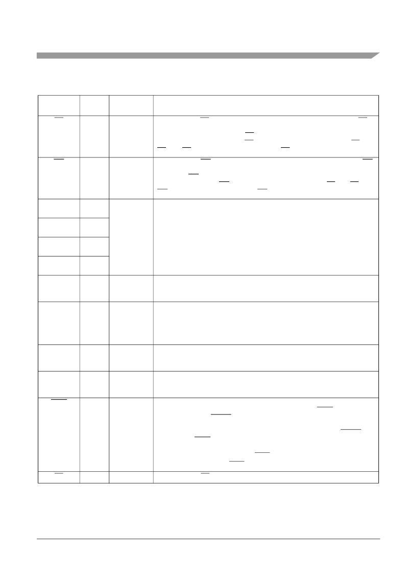
Signals and Package Information
56F826 Technical Data, Rev. 14
Freescale Semiconductor
13
RD
26
Output
Read Enable
—RD is asserted during external memory read cycles. When RD is
asserted low, pins D0–D15 become inputs and an external device is enabled
onto the device data bus. When RD is deasserted high, the external data is
latched inside the device. When RD is asserted, it qualifies the A0–A15, PS, and
DS pins. RD can be connected directly to the OE pin of a Static RAM or ROM.
WR
27
Output
Write Enable
—WR is asserted during external memory write cycles. When WR
is asserted low, pins D0–D15 become outputs and the device puts data on the
bus. When WR is deasserted high, the external data is latched inside the
external device. When WR is asserted, it qualifies the A0–A15, PS, and DS pins.
WR can be connected directly to the WE pin of a Static RAM.
TA0
(GPIOF0)
91
Input/Output
Input/Output
TA0–3
—Timer A Channels 0, 1, 2, and 3
Port F GPIO
—These four General Purpose I/O (GPIO) pins can be individually
programmed as input or output.
After reset, the default state is Quad Timer.
TA1
(GPIOF1)
90
TA2
(GPIOF2)
89
TA3
(GPIOF3)
88
TCK
100
Input
(Schmitt)
Test Clock Input
—This input pin provides a gated clock to synchronize the test
logic and shift serial data to the JTAG/OnCE port. The pin is connected internally
to a pull-down resistor.
TMS
1
Input
(Schmitt)
Test Mode Select Input
—This input pin is used to sequence the JTAG TAP
controller’s state machine. It is sampled on the rising edge of TCK and has an
on-chip pull-up resistor.
Note:
Always tie the TMS pin to V
DD
through a 2.2K resistor.
TDI
2
Input
(Schmitt)
Test Data Input
—This input pin provides a serial input data stream to the
JTAG/OnCE port. It is sampled on the rising edge of TCK and has an on-chip
pull-up resistor.
TDO
3
Output
Test Data Output
—This tri-statable output pin provides a serial output data
stream from the JTAG/OnCE port. It is driven in the Shift-IR and Shift-DR
controller states, and changes on the falling edge of TCK.
TRST
4
Input
(Schmitt)
Test Reset
—As an input, a low signal on this pin provides a reset signal to the
JTAG TAP controller. To ensure complete hardware reset, TRST should be
asserted whenever RESET is asserted. The only exception occurs in a
debugging environment when a hardware device reset is required and it is
necessary not to reset the JTAG/OnCE module. In this case, assert RESET, but
do not assert TRST. TRST must always be asserted at power-up.
Note:
in a debugging environment, TRST may be tied to V
SS
through a 1K resistor.
For normal operation, connect TRST directly to V
SS
. If the design is to be used
DE
98
Output
Debug Event
—DE provides a low pulse on recognized debug events.
Table 2-1 56F826 Signal and Package Information for the 100 Pin LQFP (Continued)
Signal
Name
Pin No.
Type
Description
相關(guān)PDF資料 |
PDF描述 |
|---|---|
| DSP56F826E | 16-bit Digital Signal Controllers |
| DSP56F826 | 16-bit Hybrid Controller(16位混合控制器) |
| DSP56F827E | 16-bit Digital Signal Controllers |
| DSP56F827FG80 | 16-bit Digital Signal Controllers |
| DSP56F827FG80E | 16-bit Digital Signal Controllers |
相關(guān)代理商/技術(shù)參數(shù) |
參數(shù)描述 |
|---|---|
| DSP56F826BU80E | 制造商:Freescale Semiconductor 功能描述:Digital Signal Processor IC DSP Type:Cor |
| DSP56F826BU80E | 制造商:Freescale Semiconductor 功能描述:DSP LQFP100 3.6V |
| DSP56F826D | 制造商:MOTOROLA 制造商全稱:Motorola, Inc 功能描述:Preliminary Technical Data DSP56F826 16-bit Digital Signal Processor |
| DSP56F826E | 制造商:FREESCALE 制造商全稱:Freescale Semiconductor, Inc 功能描述:16-bit Digital Signal Controllers |
| DSP56F826EVM | 功能描述:開發(fā)板和工具包 - 其他處理器 Evaluation Kit For DSP56F826 RoHS:否 制造商:Freescale Semiconductor 產(chǎn)品:Development Systems 工具用于評(píng)估:P3041 核心:e500mc 接口類型:I2C, SPI, USB 工作電源電壓: |
發(fā)布緊急采購(gòu),3分鐘左右您將得到回復(fù)。