- 您現(xiàn)在的位置:買賣IC網(wǎng) > PDF目錄9446 > DS4M200P+33 (Maxim Integrated Products)IC OSC CLOCK 200MHZ 10-LCCC PDF資料下載
參數(shù)資料
| 型號(hào): | DS4M200P+33 |
| 廠商: | Maxim Integrated Products |
| 文件頁數(shù): | 2/7頁 |
| 文件大小: | 0K |
| 描述: | IC OSC CLOCK 200MHZ 10-LCCC |
| 產(chǎn)品培訓(xùn)模塊: | Lead (SnPb) Finish for COTS Obsolescence Mitigation Program |
| 標(biāo)準(zhǔn)包裝: | 27 |
| 類型: | 時(shí)鐘振蕩器 |
| 頻率: | 200MHz |
| 電源電壓: | 3.135 V ~ 3.465 V |
| 電流 - 電源: | 74mA |
| 工作溫度: | -40°C ~ 85°C |
| 封裝/外殼: | 10-LCCC 裸露焊盤 |
| 包裝: | 管件 |
| 供應(yīng)商設(shè)備封裝: | 10-LCCC |
| 安裝類型: | 表面貼裝 |
DS4M125/DS4M133/DS4M200
3.3V Margining Clock Oscillator with
LVPECL/LVDS Output
2
_______________________________________________________________________________________
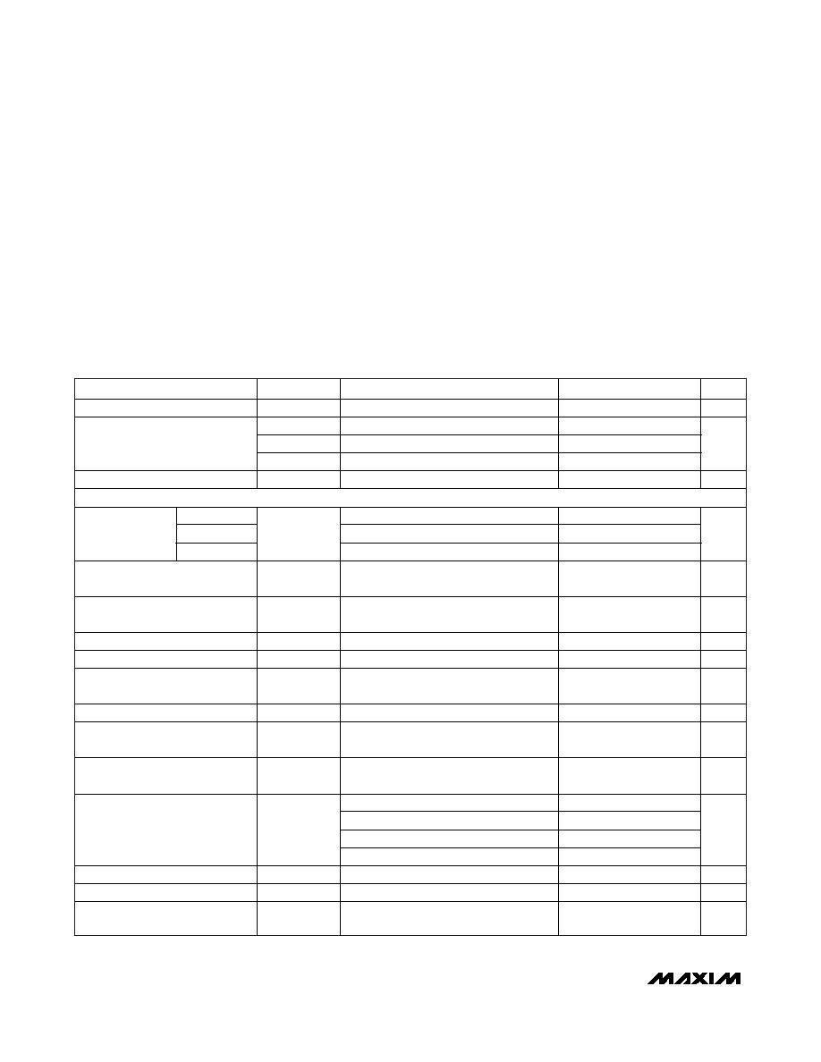
ABSOLUTE MAXIMUM RATINGS
ELECTRICAL CHARACTERISTICS
(VCC = 3.135V to 3.465V, TA = -40°C to +85°C, unless otherwise noted.) (Notes 1, 2)
Stresses beyond those listed under “Absolute Maximum Ratings” may cause permanent damage to the device. These are stress ratings only, and functional
operation of the device at these or any other conditions beyond those indicated in the operational sections of the specifications is not implied. Exposure to
absolute maximum rating conditions for extended periods may affect device reliability.
Power-Supply Voltage Range (VCC) .....................-0.3V to +4.0V
Continuous Power Dissipation (TA = +70°C) ...................330mW
Operating Temperature Range ...........................-40
°C to +85°C
Junction Temperature ......................................................+125
°C
Storage Temperature Range ...............................-55
°C to +85°C
Soldering Temperature
(3 passes max of reflow)..........................................Refer to the
IPC/JEDEC J-STD-020 Specification.
PARAMETER
SYMBOL
CONDITIONS
MIN
TYP
MAX
UNITS
Operating Voltage Range
VCC
(Note 1)
3.135
3.3
3.465
V
ICC_D
LVDS, output loaded or unloaded
52
75
ICC_PU
LVPECL, output unloaded
49
70
Operating Current
ICC_PI
LVPECL, output loaded
74
100
mA
Inactive Current
ICC_OEZ
VOE = VIL
52
85
mA
OUTPUT FREQUENCY SPECIFICATIONS
DS4M125
MS = 0, OE = 1
125
DS4M133
MS = 0, OE = 1
133.33
Frequency
DS4M200
fO
MS = 0, OE = 1
200
MHz
Frequency Stability
fTOTAL/fO
Over temperature range, aging, load,
supply, and initial tolerance (Note 3)
-50
+50
ppm
Frequency Stability Over
Temperature
fTEMP/f
VCC = 3.3V
-35
+35
ppm
Initial Tolerance
fINITIAL/fV
VCC = 3.3V, TA = +25°C
±20
ppm
Frequency Change Due to VCC
fVCC/f
VCC = 3.3V ±5%
-3
+3
ppm/V
Frequency Change Due to Load
Variation
fLOAD/fO
±10% variation in termination
resistance
±1
ppm
Aging (15 Years)
fAGING
-7
+7
ppm
Phase Jitter
JRMS
Integrated phase RMS; 12kHz to 80MHz,
VCC = 3.3V, TA = +25°C
< 0.9
ps
Accumulated Deterministic Jitter
Due to Reference Spurs
No margin 155.52MHz output
0.6
ps
10kHz
12.9
100kHz (Note 4)
26.3
200kHz (Note 4)
20.1
Accumulated Deterministic Jitter
Due to Power-Supply Noise
1MHz (Note 4)
6.4
ps
Startup Time
tSTRT
1.0
ms
Frequency Switch Time
tSWITCH
0.5
ms
Input-Voltage High (OE)
VIH
(Note 5)
0.7 x
VCC
V
相關(guān)PDF資料 |
PDF描述 |
|---|---|
| VE-B5M-IU-F2 | CONVERTER MOD DC/DC 10V 200W |
| DS4250P+ | IC OSC CLOCK 250MHZ 10-LCCC |
| M83723/72W1624Y | CONN RCPT 24POS WALL MT W/PINS |
| M83723/72W16247 | CONN RCPT 24POS WALL MT W/PINS |
| M83723/72W16246 | CONN RCPT 24POS WALL MT W/PINS |
相關(guān)代理商/技術(shù)參數(shù) |
參數(shù)描述 |
|---|---|
| DS4-M-DC12V | 制造商:AROMAT 功能描述: 制造商:Panasonic Electric Works 功能描述: |
| DS4-M-DC5V | 制造商:Panasonic Electric Works 功能描述: |
| DS4-ML2-DC12V | 制造商:Panasonic Electric Works 功能描述: |
| DS4-ML2-DC24V | 制造商:Panasonic Electric Works 功能描述: |
| DS4-ML2-DC48V | 制造商:Panasonic Electric Works 功能描述: |
發(fā)布緊急采購(gòu),3分鐘左右您將得到回復(fù)。