- 您現(xiàn)在的位置:買賣IC網(wǎng) > PDF目錄1915 > DS32512N+ (Maxim Integrated Products)IC LIU DS3/E3/STS-1 12P 484-BGA PDF資料下載
參數(shù)資料
| 型號: | DS32512N+ |
| 廠商: | Maxim Integrated Products |
| 文件頁數(shù): | 73/130頁 |
| 文件大小: | 0K |
| 描述: | IC LIU DS3/E3/STS-1 12P 484-BGA |
| 產(chǎn)品培訓(xùn)模塊: | Lead (SnPb) Finish for COTS Obsolescence Mitigation Program |
| 標(biāo)準(zhǔn)包裝: | 30 |
| 類型: | 線路接口裝置(LIU) |
| 規(guī)程: | DS3 |
| 電源電壓: | 3.135 V ~ 3.465 V |
| 安裝類型: | 表面貼裝 |
| 封裝/外殼: | 484-BGA |
| 供應(yīng)商設(shè)備封裝: | 484-BGA(23x23) |
| 包裝: | 管件 |
第1頁第2頁第3頁第4頁第5頁第6頁第7頁第8頁第9頁第10頁第11頁第12頁第13頁第14頁第15頁第16頁第17頁第18頁第19頁第20頁第21頁第22頁第23頁第24頁第25頁第26頁第27頁第28頁第29頁第30頁第31頁第32頁第33頁第34頁第35頁第36頁第37頁第38頁第39頁第40頁第41頁第42頁第43頁第44頁第45頁第46頁第47頁第48頁第49頁第50頁第51頁第52頁第53頁第54頁第55頁第56頁第57頁第58頁第59頁第60頁第61頁第62頁第63頁第64頁第65頁第66頁第67頁第68頁第69頁第70頁第71頁第72頁當(dāng)前第73頁第74頁第75頁第76頁第77頁第78頁第79頁第80頁第81頁第82頁第83頁第84頁第85頁第86頁第87頁第88頁第89頁第90頁第91頁第92頁第93頁第94頁第95頁第96頁第97頁第98頁第99頁第100頁第101頁第102頁第103頁第104頁第105頁第106頁第107頁第108頁第109頁第110頁第111頁第112頁第113頁第114頁第115頁第116頁第117頁第118頁第119頁第120頁第121頁第122頁第123頁第124頁第125頁第126頁第127頁第128頁第129頁第130頁
DS32506/DS32508/DS32512
47 of 130
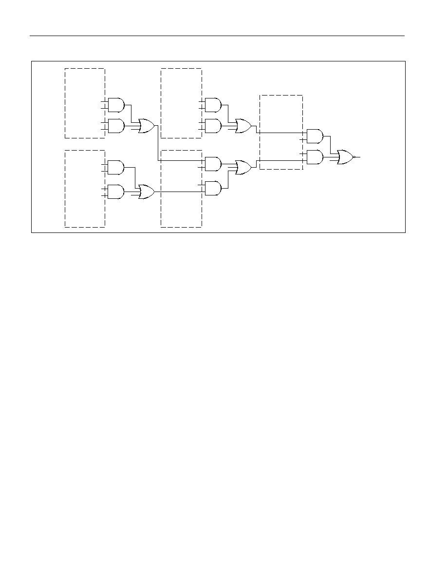
Figure 8-12. Interrupt Signal Flow
GLOBAL LATCHED
STATUS REGISTER
AND INTERRUPT
ENABLE REGISTER
INT*
GLOBAL.SRL bit
GLOBAL.SRIE bit
GLOBAL INTERRUPT
STATUS REGISTER
AND INTERRUPT
ENABLE REGISTER
GLOBAL.ISR bit
GLOBAL.ISRIE bit
BLOCK LATCHED
STATUS REGISTER
AND INTERRUPT
ENABLE REGISTER
block SRL bit
block SRIE bit
PORT INTERRUPT
STATUS REGISTER
AND INTERRUPT
ENABLE REGISTER
PORT.ISRIE bit
PORT.ISR bit
PORT.ISRIE bit
PORT.SRL bit
PORT LATCHED
STATUS REGISTER
AND INTERRUPT
ENABLE REGISTER
PORT.SRIE bit
PORT.SRL bit
PORT.SRIE bit
block SRL bit
block SRIE bit
GLOBAL.SRL bit
GLOBAL.SRIE bit
GLOBAL.ISRIE bit
GLOBAL.ISR bit
8.11 Reset and Power-Down
When only the hardware interface is enabled (IFSEL = 000 and HW = 1), the device is can be reset via the RST
pin. The transmitters of all ports can be powered down using the TPD pin, while the receivers of all ports can be
powered down using the RPD pin.
When a microprocessor interface is enabled (IFSEL
≠ 000), the device presents a number of reset and power down
options. The device can be reset at a global level via the GLOBAL.CR1:RST bit or the RST pin, and at the port
level via the PORT.CR1:RST bit. Each port can be powered down via the PORT.CR1:TPD and RPD bits. The
JTAG logic is reset by the
JTRST pin.
The external RST pin and the global reset bit (GLOBAL.CR1:RST) are combined to create an internal global reset
signal. The global reset signal resets all the status and control registers on the chip (except the GLOBAL.CR1:RST
bit), to their default values. It also resets all flip-flops in the global logic (including the CLAD block) and port logic to
their reset values. The GLOBAL.CR1:RST bit stays set after a one is written to it. It is reset to zero when a zero is
written to it or when the external RST pin is active.
At the port level, the global reset signal combines with the port reset bit (PORT.CR1:RST) to create a port reset
signal. The port reset signal resets all the status and control registers in the port (except PORT.CR1:RST bit) to
their default values. It also resets all flip-flops in the port logic to their reset values. The port reset bit
(PORT.CR1:RST) stays set after a one is written to it. It is reset to zero when a zero is written to it or when the
global reset signal is active.
The data path reset (RSTDP) resets all of the same registers and flip-flops as the “general” reset (RST), except for
the control registers. This allows the device to be programmed while the data path logic is in reset. It is
recommended that a port be placed in data path reset during configuration changes.
The global data path reset bit (GLOBAL.CR1:RSTDP) is set to one when the global reset signal is active. This bit is
cleared when a zero is written to it while the global reset signal is inactive. The global data path reset resets all of
the data path registers and flip-flops on the chip.
The port data path reset bit (PORT.CR1:RSTDP) is set to one when the port reset signal is active. It is cleared
when a zero is written to it while the port reset signal is inactive. The port data path reset resets all of the port logic
data path registers and flip-flops.
相關(guān)PDF資料 |
PDF描述 |
|---|---|
| DS3254N+ | IC LIU DS3/E3/STS-1 144-CSBGA |
| DS33M33N+ | IC MAPPER ETHERNET 256CSBGA |
| DS33R11+CJ2 | IC ETH TXRX T1/E1/J1 256-BGA |
| DS33R41+ | IC TXRX ETHERNET MAP 400-BGA |
| DS33W11DK+ | IC MAPPING ETHERNET 256-CSBGA |
相關(guān)代理商/技術(shù)參數(shù) |
參數(shù)描述 |
|---|---|
| DS32512N# | 功能描述:網(wǎng)絡(luò)控制器與處理器 IC 12-Port DS3/E3/STS-1 Line Interface Unit RoHS:否 制造商:Micrel 產(chǎn)品:Controller Area Network (CAN) 收發(fā)器數(shù)量: 數(shù)據(jù)速率: 電源電流(最大值):595 mA 最大工作溫度:+ 85 C 安裝風(fēng)格:SMD/SMT 封裝 / 箱體:PBGA-400 封裝:Tray |
| DS32512N+ | 功能描述:網(wǎng)絡(luò)控制器與處理器 IC 12-Port DS3/E3/STS-1 Line Interface Unit RoHS:否 制造商:Micrel 產(chǎn)品:Controller Area Network (CAN) 收發(fā)器數(shù)量: 數(shù)據(jù)速率: 電源電流(最大值):595 mA 最大工作溫度:+ 85 C 安裝風(fēng)格:SMD/SMT 封裝 / 箱體:PBGA-400 封裝:Tray |
| DS32512NA2 | 制造商:Maxim Integrated Products 功能描述:DS32512 X12 DS3/E3 LIU REVA2 IND - Rail/Tube |
| DS32512NW | 功能描述:網(wǎng)絡(luò)控制器與處理器 IC RoHS:否 制造商:Micrel 產(chǎn)品:Controller Area Network (CAN) 收發(fā)器數(shù)量: 數(shù)據(jù)速率: 電源電流(最大值):595 mA 最大工作溫度:+ 85 C 安裝風(fēng)格:SMD/SMT 封裝 / 箱體:PBGA-400 封裝:Tray |
| DS32512W | 功能描述:網(wǎng)絡(luò)控制器與處理器 IC RoHS:否 制造商:Micrel 產(chǎn)品:Controller Area Network (CAN) 收發(fā)器數(shù)量: 數(shù)據(jù)速率: 電源電流(最大值):595 mA 最大工作溫度:+ 85 C 安裝風(fēng)格:SMD/SMT 封裝 / 箱體:PBGA-400 封裝:Tray |
發(fā)布緊急采購,3分鐘左右您將得到回復(fù)。