- 您現(xiàn)在的位置:買賣IC網(wǎng) > PDF目錄97868 > DS229E (DALLAS SEMICONDUCTOR) LINE TRANSCEIVER, PDSO20 PDF資料下載
參數(shù)資料
| 型號(hào): | DS229E |
| 廠商: | DALLAS SEMICONDUCTOR |
| 元件分類: | Line Driver or Receiver |
| 英文描述: | LINE TRANSCEIVER, PDSO20 |
| 封裝: | TSSOP-20 |
| 文件頁數(shù): | 4/11頁 |
| 文件大小: | 1042K |
| 代理商: | DS229E |
MAX14983E
Enhanced 1:2 VGA Mux with
Monitor Detection and Priority Port Logic
2
Maxim Integrated
(Voltages referenced to GND.)
VCC, S5V1, S5V2, SDA_, SCL_, REF, MD_,
EN_, MDOR .........................................................-0.3V to +6V
HSYNC_, VSYNC_, R_, G_, B_................. -0.3V to (VCC + 0.3V)
Continuous Current Through R_, G_, B_ Switches......... Q50mA
Continuous Current Through SDA_, SCL_ Switches ...... Q50mA
Continuous Current Through S5V_ ............................... Q750mA
Peak Current Through R_, G_, B_, SDA_, SCL_
(10% duty cycle) ....................................................... Q100mA
Continuous Power Dissipation (TA = +70NC)
TQFN (derate 34.5mW/NC above +70NC)...............2758.6mW
Operating Temperature Range.......................... -40NC to +85NC
Junction Temperature .....................................................+150NC
Storage Temperature Range............................ -65NC to +150NC
Lead Temperature (soldering, 10s) ...............................+300NC
Soldering Temperature (reflow) ......................................+260NC
TQFN
Junction-to-Ambient Thermal Resistance (BJA) ..........29NC/W
Junction-to-Case Thermal Resistance (BJC) ..............1.7NC/W
ABSOLUTE MAXIMUM RATINGS
Note 1: Package thermal resistances were obtained using the method described in JEDEC specification JESD51-7, using a four-layer
board. For detailed information on package thermal considerations, refer to www.maximintegrated.com/thermal-tutorial.
Stresses beyond those listed under “Absolute Maximum Ratings” may cause permanent damage to the device. These are stress ratings only, and functional opera-
tion of the device at these or any other conditions beyond those indicated in the operational sections of the specifications is not implied. Exposure to absolute
maximum rating conditions for extended periods may affect device reliability.
PACKAGE THERMAL CHARACTERISTICS (Note 1)
ELECTRICAL CHARACTERISTICS
(VCC = +5V Q5%, TA = -40NC to +85NC, unless otherwise noted. Typical values are at VCC = +5V, TA = +25NC.) (Note 2)
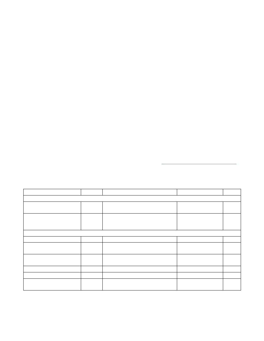
PARAMETER
SYMBOL
CONDITIONS
MIN
TYP
MAX
UNITS
POWER SUPPLY
Quiescent Current
IQ
VCC = 5.25V, VEN1 = VEN2 = VCC, REF
unconnected
50
150
F
A
Operating Current
ICC
HSYNC0 = 50kHz, VSYNC0 = 60Hz 10%
duty cycle, RL on SYNC outputs = 2kI,
REF unconnected
1.5
2.7
mA
5V SWITCH (S5V1, S5V2 OUTPUTS)
S5V_ Voltage Drop
VS5V
IOUT = 55mA
0.3
V
Reverse Leakage Current
IL
VCC = 0V, VEN1 = VEN2 = 0V, VS5V1 =
VS5V2 = 5.25V, no load on S5V1 or S5V2
10
F
A
Pulldown Resistor
RS5V1,
RS5V2
VS5V1 = VS5V2 = 1V, VEN1 = VEN2 = VCC
250
I
Output Current Limit
ILIM
55
300
500
mA
Thermal-Shutdown Threshold
TSHDN
+150
N
C
Thermal-Shutdown Hysteresis
TSHDN_
HYS
25
N
C
相關(guān)PDF資料 |
PDF描述 |
|---|---|
| DS229N | LINE TRANSCEIVER, PDIP20 |
| DS229SN | LINE TRANSCEIVER, PDSO20 |
| DS2151Q | DATACOM, FRAMER, PQCC44 |
| DS229S | LINE TRANSCEIVER, PDSO20 |
| DS232AE | LINE TRANSCEIVER, PDSO20 |
相關(guān)代理商/技術(shù)參數(shù) |
參數(shù)描述 |
|---|---|
| DS229E/T&R | 功能描述:RS-232接口集成電路 RoHS:否 制造商:Exar 數(shù)據(jù)速率:52 Mbps 工作電源電壓:5 V 電源電流:300 mA 工作溫度范圍:- 40 C to + 85 C 安裝風(fēng)格:SMD/SMT 封裝 / 箱體:LQFP-100 封裝: |
| DS229E+ | 功能描述:RS-232接口集成電路 RoHS:否 制造商:Exar 數(shù)據(jù)速率:52 Mbps 工作電源電壓:5 V 電源電流:300 mA 工作溫度范圍:- 40 C to + 85 C 安裝風(fēng)格:SMD/SMT 封裝 / 箱體:LQFP-100 封裝: |
| DS229E+T&R | 制造商:Maxim Integrated Products 功能描述:IC TXRX TRI 5V RS-232 20-TSSOP |
| DS229E+T&R | 功能描述:RS-232接口集成電路 RoHS:否 制造商:Exar 數(shù)據(jù)速率:52 Mbps 工作電源電壓:5 V 電源電流:300 mA 工作溫度范圍:- 40 C to + 85 C 安裝風(fēng)格:SMD/SMT 封裝 / 箱體:LQFP-100 封裝: |
| DS229EN | 功能描述:RS-232接口集成電路 RoHS:否 制造商:Exar 數(shù)據(jù)速率:52 Mbps 工作電源電壓:5 V 電源電流:300 mA 工作溫度范圍:- 40 C to + 85 C 安裝風(fēng)格:SMD/SMT 封裝 / 箱體:LQFP-100 封裝: |
發(fā)布緊急采購,3分鐘左右您將得到回復(fù)。