- 您現(xiàn)在的位置:買賣IC網(wǎng) > Datasheet目錄39 > DS1842N+T&R (Maxim Integrated)IC CURRENT MONITOR 14TDFN Datasheet資料下載
參數(shù)資料
| 型號(hào): | DS1842N+T&R |
| 廠商: | Maxim Integrated |
| 文件頁數(shù): | 2/7頁 |
| 文件大小: | 210K |
| 描述: | IC CURRENT MONITOR 14TDFN |
| 產(chǎn)品培訓(xùn)模塊: | Lead (SnPb) Finish for COTS Obsolescence Mitigation Program |
| 標(biāo)準(zhǔn)包裝: | 2,500 |
| 功能: | 電流監(jiān)控器 |
| 工作溫度: | -40°C ~ 85°C |
| 安裝類型: | 表面貼裝 |
| 封裝/外殼: | 14-WFDFN 裸露焊盤 |
| 供應(yīng)商設(shè)備封裝: | 14-TDFN-EP(3x3) |
| 包裝: | 帶卷 (TR) |
76V, APD, Bias Output Stage with
Current Monitoring
2 _______________________________________________________________________________________
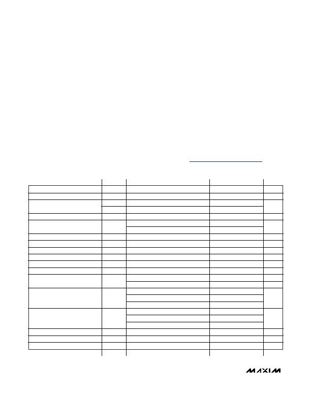
ABSOLUTE MAXIMUM RATINGS
ELECTRICAL CHARACTERISTICS
(T
A
= -40癈 to +85癈, unless otherwise noted.)
Stresses beyond those listed under
Absolute Maximum Ratings
may cause permanent damage to the device. These are stress ratings only, and functional
operation of the device at these or any other conditions beyond those indicated in the operational sections of the specifications is not implied. Exposure to
absolute maximum rating conditions for extended periods may affect device reliability.
Note 2: Rising MIROUT transition from 10?/SPAN>A to 1mA; V
MIRIN
= 40V, 2.5k?load.
Note 3: Guaranteed by design; not production tested.
Voltage Range on GATE and CLAMP
Relative to GND...................................................-0.3V to +12V
Voltage Range on MIRIN, MIROUT,
MIR1, and MIR2 Relative to GND........................-0.3V to +80V
Voltage Range on LX Relative to GND...................-0.3V to +85V
Continuous Power Dissipation (T
A
= +70癈)
TDFN (derate 24.4mW/癈 above +70癈).................1951.2mW
Operating Junction Temperature Range...........-40癈 to +150癈
Storage Temperature Range.............................-55癈 to +135癈
Lead Temperature (soldering, 10s).................................+300癈
Soldering Temperature (reflow).......................................+260癈
PACKAGE THERMAL CHARACTERISTICS (Note 1)
TDFN
Junction-to-Ambient Thermal Resistance (?/DIV>
JA
) ............41癈/W
Junction-to-Case Thermal Resistance (?/DIV>
JC
)...................8癈/W
PARAMETER
SYMBOL
CONDITIONS
MIN
TYP
MAX UNITS
Switching Frequency
f
SW
0
1.2
MHz
C
GATE
V
GS
= 0V, V
DS
= 25V
40
FET Capacitance
C
LX
f
SW
= 1MHz
90
pF
FET Gate Resistance
R
G
22
V
GS
= 3V, I
D
= 170mA
4.6
10
FET On-Resistance
R
DSON
V
GS
= 10V, I
D
= 170mA
3.7
8
GATE Voltage
V
GS
0
11
V
Switching Current
I
LX
Duty cycle = 10%, f
SW
= 100kHz
680
mA
LX Voltage
V
LX
80
V
LX Leakage
I
IL(LX)
V
GATE
= 0V, V
LX
= 76V
-1
+1
糀
CLAMP Voltage
V
CLAMP
0
11
V
CLAMP Threshold
V
CLT
2
4
7
V
CLAMP = low
1.75
2.6
4
mA
Maximum MIROUT Current
I
MIROUT
CLAMP = high
10
糀
I
MIROUT
= 1mA
0.095 0.100 0.105
I
MIROUT
= 1糀
0.094 0.100 0.106
MIR1 to MIROUT Ratio
K
MIR1
15V < V
MIRIN
< 76V
A/A
I
MIROUT
= 1mA
0.190 0.200 0.210
I
MIROUT
= 1糀
0.188 0.200 0.212
MIR2 to MIROUT Ratio
K
MIR2
15V < V
MIRIN
< 76V
A/A
MIR1, MIR2 Rise Time (20%/80%)
t
RC
(Note 2)
30
ns
Shutdown Temperature
T
SHDN
(Note 3)
+150
癈
Leakage on GATE and CLAMP
I
IL
-1
+1
糀
Note 1: Package thermal resistances were obtained using the method described in JEDEC specification JESD51-7, using a four-layer
board. For detailed information on package thermal considerations, refer to www.maxim-ic.com/thermal-tutorial
.
相關(guān)PDF資料 |
PDF描述 |
|---|---|
| DS18B20+PAR | IC THERM MICROLAN PROG-RES TO-92 |
| DS18B20Z/T&R | IC THERM MICROLAN PROG-RES 8SOIC |
| DS2740U+T&R | IC CURRENT GAUGE(15BIT) 8UMAX |
| DS28EA00U+T&R | IC THERMOMETER 1-WIRE 8-USOP |
| DS3920T-001+ | IC CURRENT MIRROR 5:1 SOT23-6 |
相關(guān)代理商/技術(shù)參數(shù) |
參數(shù)描述 |
|---|---|
| DS1843 | 制造商:MAXIM 制造商全稱:Maxim Integrated Products 功能描述:Fast Sample-and-Hold Circuit |
| DS1843_12 | 制造商:MAXIM 制造商全稱:Maxim Integrated Products 功能描述:Fast Sample-and-Hold Circuit |
| DS1843D | 制造商:MAXIM 制造商全稱:Maxim Integrated Products 功能描述:Fast Sample-and-Hold Circuit |
| DS1843D TRL | 制造商:MAXIM 制造商全稱:Maxim Integrated Products 功能描述:Fast Sample-and-Hold Circuit |
| DS1843D+ | 功能描述:采樣&保持放大器 Fast Sample & Hold Circuit RoHS:否 制造商:Texas Instruments 通道數(shù)量:2 捕獲時(shí)間:20 us 電源電壓-最大:18 V 最大工作溫度:+ 85 C 最小工作溫度:- 25 C 安裝風(fēng)格: 封裝 / 箱體:SOIC-14 封裝:Tube |
發(fā)布緊急采購,3分鐘左右您將得到回復(fù)。