- 您現(xiàn)在的位置:買賣IC網(wǎng) > PDF目錄211934 > DPS512X32MFY3-35B 512K X 32 MULTI DEVICE SRAM MODULE, 35 ns, QMA68 PDF資料下載
參數(shù)資料
| 型號: | DPS512X32MFY3-35B |
| 元件分類: | SRAM |
| 英文描述: | 512K X 32 MULTI DEVICE SRAM MODULE, 35 ns, QMA68 |
| 封裝: | LEADLESS, STACK, SLCC-68 |
| 文件頁數(shù): | 3/8頁 |
| 文件大小: | 811K |
| 代理商: | DPS512X32MFY3-35B |
Dense-Pac Microsystems, Inc.
DPS512X32MFn3
+5V
255
480
CL*
DOUT
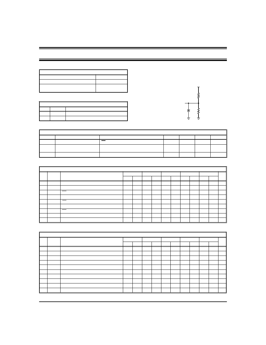
Figure 1. Output Load
* Including Probe and Jig Capacitance.
OUTPUT LOAD
Load
CL
Parameters Measured
1
100pF
except tLZ, tHZ, tOHZ, tOLZ, and tWHZ
2
5pF
tLZ, tHZ, tOHZ, tOLZ, and tWHZ
AC TEST CONDITIONS
Input Pulse Levels
0V to 3.0V
Input Pulse Rise and Fall Times
5ns
Input and Output
Timing Reference Levels
1.5V
Data Retention AC Characteristics 8
Symbol
Parameter
Test Conditions
Min.
Typ.
Max.
Unit
VDR
VDD for Data Retention
CE
≥ VDR -0.2V
2.0
-
V
VCDR
Chip Disable to
Data Retention Time
See Data Retention Waveform
0
-
ns
tR
Operation Recovery Time
See Data Retention Waveform
5
-
ms
AC OPERATING CONDITIONS AND CHARACTERISTICS - READ CYCLE: Over operating ranges
No. Symbol
Parameter
20ns*
25ns
30ns
35ns
45ns
Unit
Min.
Max.
Min.
Max. Min.
Max.
Min.
Max.
Min. Max.
1
tRC
Read Cycle Time
20
25
30
35
45
ns
2
tAA
Address Access Time
20
25
30
35
45
ns
3
tCO
CE to Output Valid
20
25
30
35
45
ns
4
tOE
Output Enable to Output Valid
10
12
15
20
25
ns
5
tLZ
CE to Output in LOW-Z 4, 5
3
ns
6
tOLZ
Output Enable to Output in LOW-Z 4, 5
0
ns
7
tHZ
CE to Output in HIGH-Z 4, 5
8
10
15
20
25
ns
8
tOHZ
Output Enable to Output in HIGH-Z 4, 5
0
8
0
10
0
15
0
20
0
25
ns
9
tOH
Output Hold from Address Change
4
5
ns
AC OPERATING CONDITIONS AND CHARACTERISTICS - WRITE CYCLE 6, 7: Over operating ranges
No. Symbol
Parameter
20ns*
25ns
30ns
35ns
45ns
Unit
Min.
Max. Min.
Max.
Min.
Max.
Min. Max.
10
tWC
Write Cycle Time
20
25
30
35
45
ns
11
tAW
Address Valid to End of Write
13
15
20
25
35
ns
12
tCW
Chip Enable to End of Write
13
15
20
25
35
ns
13
tAS
Address Set-Up Time **
3
ns
14
tWP
Write Pulse Width
13
15
20
25
35
ns
15
tWR
Write Recovery Time
0
ns
16
tWHZ
Write Enable to Output in HIGH-Z 4, 5
0
8
0
10
0
12
0
15
0
20
ns
17
tDW
Data to Write Time Overlap
9
10
12
15
20
ns
18
tDH
Data Hold from Write Time
0
ns
19
tOW
Output Active from End of Write
3
ns
* Available in Commercial and Industrial Grade Only.
30A154-04
REV. B
3
相關(guān)PDF資料 |
PDF描述 |
|---|---|
| DPZ128X16IJY-25M | 128K X 16 FLASH 12V PROM MODULE, 250 ns, QCC48 |
| DT22J31S102QA7 | ROCKER SWITCH, DPST, LATCHED, THROUGH HOLE-STRAIGHT |
| DT22J2GB215NQA | ROCKER SWITCH, DPST, LATCHED, PANEL MOUNT |
| DT22J2GB215NQF8 | ROCKER SWITCH, DPST, LATCHED, PANEL MOUNT |
| DT22J2GG202HQH7 | ROCKER SWITCH, DPST, LATCHED, THROUGH HOLE-STRAIGHT |
相關(guān)代理商/技術(shù)參數(shù) |
參數(shù)描述 |
|---|---|
| DPS512X32MFY3-35C | 制造商:未知廠家 制造商全稱:未知廠家 功能描述:x32 SRAM Module |
| DPS512X32MFY3-35I | 制造商:未知廠家 制造商全稱:未知廠家 功能描述:x32 SRAM Module |
| DPS512X32MFY3-35M | 制造商:未知廠家 制造商全稱:未知廠家 功能描述:x32 SRAM Module |
| DPS512X32MFY3-45B | 制造商:未知廠家 制造商全稱:未知廠家 功能描述:x32 SRAM Module |
| DPS512X32MFY3-45C | 制造商:未知廠家 制造商全稱:未知廠家 功能描述:x32 SRAM Module |
發(fā)布緊急采購,3分鐘左右您將得到回復(fù)。