- 您現(xiàn)在的位置:買賣IC網(wǎng) > PDF目錄376722 > DJIXFLCD0QE001 (Intel Corp.) Advanced 8-Port 10/100 Mbps PHY Transceivers PDF資料下載
參數(shù)資料
| 型號(hào): | DJIXFLCD0QE001 |
| 廠商: | Intel Corp. |
| 英文描述: | Advanced 8-Port 10/100 Mbps PHY Transceivers |
| 中文描述: | 先進(jìn)的8端口10/100 Mbps的物理層收發(fā)器 |
| 文件頁(yè)數(shù): | 209/226頁(yè) |
| 文件大小: | 1575K |
| 代理商: | DJIXFLCD0QE001 |
第1頁(yè)第2頁(yè)第3頁(yè)第4頁(yè)第5頁(yè)第6頁(yè)第7頁(yè)第8頁(yè)第9頁(yè)第10頁(yè)第11頁(yè)第12頁(yè)第13頁(yè)第14頁(yè)第15頁(yè)第16頁(yè)第17頁(yè)第18頁(yè)第19頁(yè)第20頁(yè)第21頁(yè)第22頁(yè)第23頁(yè)第24頁(yè)第25頁(yè)第26頁(yè)第27頁(yè)第28頁(yè)第29頁(yè)第30頁(yè)第31頁(yè)第32頁(yè)第33頁(yè)第34頁(yè)第35頁(yè)第36頁(yè)第37頁(yè)第38頁(yè)第39頁(yè)第40頁(yè)第41頁(yè)第42頁(yè)第43頁(yè)第44頁(yè)第45頁(yè)第46頁(yè)第47頁(yè)第48頁(yè)第49頁(yè)第50頁(yè)第51頁(yè)第52頁(yè)第53頁(yè)第54頁(yè)第55頁(yè)第56頁(yè)第57頁(yè)第58頁(yè)第59頁(yè)第60頁(yè)第61頁(yè)第62頁(yè)第63頁(yè)第64頁(yè)第65頁(yè)第66頁(yè)第67頁(yè)第68頁(yè)第69頁(yè)第70頁(yè)第71頁(yè)第72頁(yè)第73頁(yè)第74頁(yè)第75頁(yè)第76頁(yè)第77頁(yè)第78頁(yè)第79頁(yè)第80頁(yè)第81頁(yè)第82頁(yè)第83頁(yè)第84頁(yè)第85頁(yè)第86頁(yè)第87頁(yè)第88頁(yè)第89頁(yè)第90頁(yè)第91頁(yè)第92頁(yè)第93頁(yè)第94頁(yè)第95頁(yè)第96頁(yè)第97頁(yè)第98頁(yè)第99頁(yè)第100頁(yè)第101頁(yè)第102頁(yè)第103頁(yè)第104頁(yè)第105頁(yè)第106頁(yè)第107頁(yè)第108頁(yè)第109頁(yè)第110頁(yè)第111頁(yè)第112頁(yè)第113頁(yè)第114頁(yè)第115頁(yè)第116頁(yè)第117頁(yè)第118頁(yè)第119頁(yè)第120頁(yè)第121頁(yè)第122頁(yè)第123頁(yè)第124頁(yè)第125頁(yè)第126頁(yè)第127頁(yè)第128頁(yè)第129頁(yè)第130頁(yè)第131頁(yè)第132頁(yè)第133頁(yè)第134頁(yè)第135頁(yè)第136頁(yè)第137頁(yè)第138頁(yè)第139頁(yè)第140頁(yè)第141頁(yè)第142頁(yè)第143頁(yè)第144頁(yè)第145頁(yè)第146頁(yè)第147頁(yè)第148頁(yè)第149頁(yè)第150頁(yè)第151頁(yè)第152頁(yè)第153頁(yè)第154頁(yè)第155頁(yè)第156頁(yè)第157頁(yè)第158頁(yè)第159頁(yè)第160頁(yè)第161頁(yè)第162頁(yè)第163頁(yè)第164頁(yè)第165頁(yè)第166頁(yè)第167頁(yè)第168頁(yè)第169頁(yè)第170頁(yè)第171頁(yè)第172頁(yè)第173頁(yè)第174頁(yè)第175頁(yè)第176頁(yè)第177頁(yè)第178頁(yè)第179頁(yè)第180頁(yè)第181頁(yè)第182頁(yè)第183頁(yè)第184頁(yè)第185頁(yè)第186頁(yè)第187頁(yè)第188頁(yè)第189頁(yè)第190頁(yè)第191頁(yè)第192頁(yè)第193頁(yè)第194頁(yè)第195頁(yè)第196頁(yè)第197頁(yè)第198頁(yè)第199頁(yè)第200頁(yè)第201頁(yè)第202頁(yè)第203頁(yè)第204頁(yè)第205頁(yè)第206頁(yè)第207頁(yè)第208頁(yè)當(dāng)前第209頁(yè)第210頁(yè)第211頁(yè)第212頁(yè)第213頁(yè)第214頁(yè)第215頁(yè)第216頁(yè)第217頁(yè)第218頁(yè)第219頁(yè)第220頁(yè)第221頁(yè)第222頁(yè)第223頁(yè)第224頁(yè)第225頁(yè)第226頁(yè)
LXT9785 and LXT9785E Advanced 8-Port 10/100 Mbps PHY Transceivers
Datasheet
Document Number: 249241
Revision Number: 007
Revision Date: August 28, 2003
211
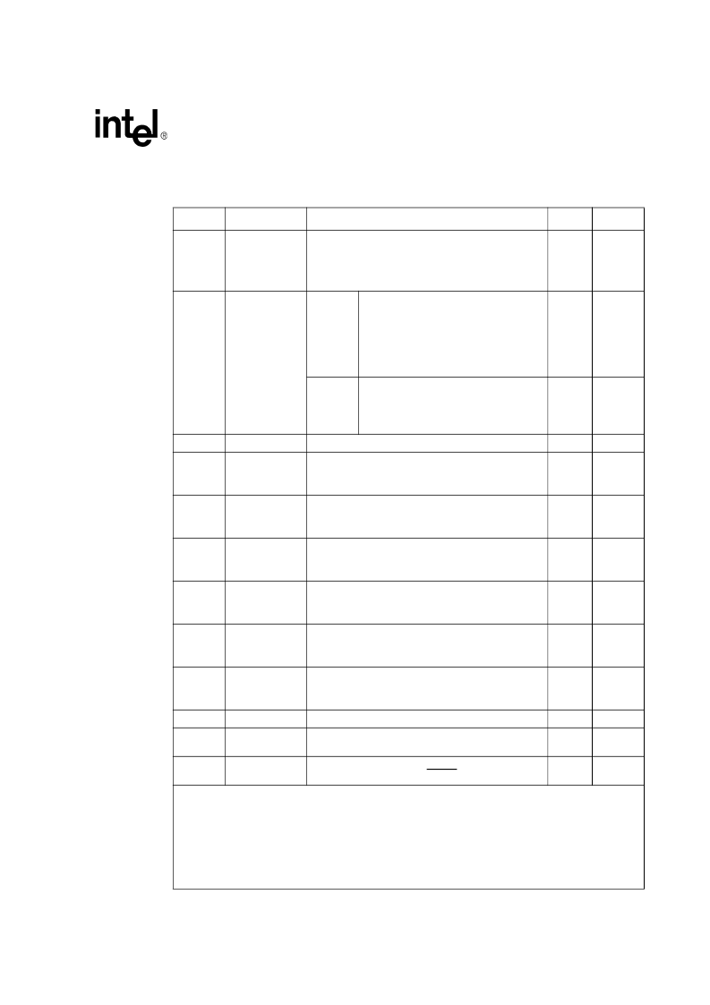
Table 94. Interrupt Enable Register (Address 18, Hex 12)
Bit
Name
Description
Type
1
Default
15:14
2
RxFIFO Initial
Fill
00 =Reserved
01 =Low, 16 bits
10 =Normal, 32 bits (default)
11 = Jumbo packets, 128 bits
R/W
LSHR
4,5
13
SFD Frame
Alignment
(RxDV asserts
with CRS when
enabled)
10 Mbps
When Register bit 16.5 = 1, preamble is
not suppressed.
R/W
0
0 = Disabled
1 = Enabled
When Register bit 16.5 = 0, SFD is always
aligned, and preamble is suppressed.
100 Mbps
0 = Disabled
1 = Enabled
R/W
0
When enabled, all but one byte of
preamble is suppressed.
12:9
Reserved
Write as 0, ignore on Read
R/W
0000
8
CNTRMSK
Mask for Counter Full
0 = Do not allow event to cause interrupt
1 = Enable event to cause interrupt
R/W
0
7
ANMSK
Mask for Auto-Negotiate Complete
0 = Do not allow event to cause interrupt
1 = Enable event to cause interrupt
R/W
0
6
SPEEDMSK
Mask for Speed Interrupt
0 = Do not allow event to cause interrupt
1 = Enable event to cause interrupt
R/W
0
5
DUPLEXMSK
Mask for Duplex Interrupt
0 = Do not allow event to cause interrupt
1 = Enable event to cause interrupt
R/W
0
4
LINKMSK
Mask for Link Status Interrupt
0 = Do not allow event to cause interrupt
1 = Enable event to cause interrupt
R/W
0
3
ISOLMSK
Mask for Isolate Interrupt
0 = Do not allow event to cause interrupt
1 = Enable event to cause interrupt
R/W
0
2
Reserved
Write as 0, ignore on Read
R/W
0
1
INTEN
0 = Disable interrupts on this port
1 = Enable interrupts on this port
R/W
0
0
TINT
0 = Normal operation
1 = Test force interrupt on MDINT
R/W
0
1. R/W = Read/Write
2. In 10 Mbps operation, Register bit 18.13 = 1 cannot be used when Register bits 18.15:14 = “11” and in
RMII mode, Registers bits 18.15:14 = “11” or “10” cannot be used because the minimum Inter Gap Packet
becomes less than specified in the *IEEE 802.3 specification.
3. SFD Frame Alignment is applicable to SMII and SS-SMII only.
4.
LSHR = Default value is derived from a single device input pin state or a group of device input pin states as
the pin(s) are latched at startup or hardware reset
5. Default values are set by hardware configuration pins FIFOSEL1 and FIFOSEL0 (see
Table 17, “Intel
LXT9785/LXT9785E Receive FIFO Depth Considerations” on page 50
).
相關(guān)PDF資料 |
PDF描述 |
|---|---|
| DJIXFLCD0SE000 | Advanced 8-Port 10/100 Mbps PHY Transceivers |
| DJIXFLCD0SE001 | Advanced 8-Port 10/100 Mbps PHY Transceivers |
| DJIXFLED0QE000 | Advanced 8-Port 10/100 Mbps PHY Transceivers |
| DJIXFLED0QE001 | Advanced 8-Port 10/100 Mbps PHY Transceivers |
| DJIXFLED0SE000 | Advanced 8-Port 10/100 Mbps PHY Transceivers |
相關(guān)代理商/技術(shù)參數(shù) |
參數(shù)描述 |
|---|---|
| DJIXFLCD0SE000 | 制造商:INTEL 制造商全稱:Intel Corporation 功能描述:Advanced 8-Port 10/100 Mbps PHY Transceivers |
| DJIXFLCD0SE001 | 制造商:INTEL 制造商全稱:Intel Corporation 功能描述:Advanced 8-Port 10/100 Mbps PHY Transceivers |
| DJIXFLED0QE000 | 制造商:INTEL 制造商全稱:Intel Corporation 功能描述:Advanced 8-Port 10/100 Mbps PHY Transceivers |
| DJIXFLED0QE001 | 制造商:INTEL 制造商全稱:Intel Corporation 功能描述:Advanced 8-Port 10/100 Mbps PHY Transceivers |
| DJIXFLED0SE000 | 制造商:INTEL 制造商全稱:Intel Corporation 功能描述:Advanced 8-Port 10/100 Mbps PHY Transceivers |
發(fā)布緊急采購(gòu),3分鐘左右您將得到回復(fù)。