- 您現(xiàn)在的位置:買賣IC網(wǎng) > PDF目錄374163 > CS235GDWR18 (ZF Electronics Corporation) System Photoelectric Smoke Detector PDF資料下載
參數(shù)資料
| 型號(hào): | CS235GDWR18 |
| 廠商: | ZF Electronics Corporation |
| 英文描述: | System Photoelectric Smoke Detector |
| 中文描述: | 系統(tǒng)光電感煙探測器 |
| 文件頁數(shù): | 2/6頁 |
| 文件大?。?/td> | 147K |
| 代理商: | CS235GDWR18 |
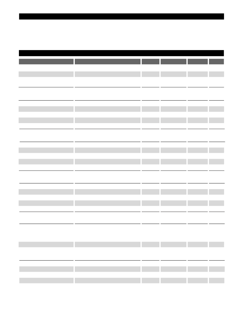
Electrical Characteristics: T
A
= 25C, unless otherwise stated.
PARAMETER
TEST CONDITIONS
MIN
TYP
MAX
UNIT
C
2
Absolute Maximum Ratings
Lead Temperature Soldering
Wave Solder (through hole styles only).....................................................................................10 sec. max, 260C peak
Reflow (SMD styles only)......................................................................................60 sec. max above 183C, 230C peak
Storage Temperature Range ..................................................................................................................................-65C to 150C
Absolute Maximum Voltage
Output Latch Current
Operation Temperature
Range, T
A
(pin 3)
38
100
70
V
mA
C
0
I
24V System (C2 = 100 μF, R7 = 12 M)
Operating Voltage
Average Supply Current
Peak Supply Current
Peak Supply Current
Regulator Voltage
(pin 3)
V (pin 3) = 22.5V
V (pin 3) = 22.5V )(non òspeed upó)
V (pin 16) = 12V )(òspeed upó)
(pin 16)
13.8
22.5
35
35
60
100
350
15.7
V
μA
μA
μA
V
150
12.8
I
12V System (C2 = 150μF, R7 = 12M)
Operating Voltage
Average Supply Current
Peak Supply Current
Peak Supply Current
Regulator Voltage
(pin 3)
V (pin 3) = 12V
V (pin 3) = 12V (non òspeed upó)
V (pin 16) = 8V (òspeed upó mode)
(pin 16) (V pin 3 = 12V)
8.7
12
V
μA
μA
μA
V
60
100
350
11.85
I
Oscillator
Output Frequency
Sink Current
Source Current
High Trip Point Voltage
Low Trip Point Voltage
R6 = 18k, C3 = .0068μF
(pin 14)
(pin 14)
(pin 14)
(pin 14)
2.1
16
19
1.8
1.2
3.3
26
26
1.9
1.4
4.4
35
32
2.2
1.5
kHz
μA
μA
V
V
I
LED Drive (Detector LED and Status LED)
Source Current (pin 15)
Detector LED
Status LED (alarm)
Regulator Voltage (pin 15)
R8=36
V IR LED = 1.156V
V Status LED = 1.99V
I
SOURCE
= 30mA
20
10
3.7
30
40
mA
mA
V
4.4
5.2
I
Amplifier A1
Fixed Gain
Input Current B
1
Input Current B
2
Input current (B
1
-B
2
)
26
500
500
dB
nA
nA
nA
(pin 5)
(pin 6)
1000
1000
250
相關(guān)PDF資料 |
PDF描述 |
|---|---|
| CS235 | System Photoelectric Smoke Detector |
| CS235GN18 | System Photoelectric Smoke Detector |
| CS2516KN8 | Pulse-Load Battery Monitor |
| CS2516 | Pulse-Load Battery Monitor |
| CS2516KD8 | Pulse-Load Battery Monitor |
相關(guān)代理商/技術(shù)參數(shù) |
參數(shù)描述 |
|---|---|
| CS235GN18 | 制造商:CHERRY 制造商全稱:CHERRY 功能描述:System Photoelectric Smoke Detector |
| CS-235N18 | 制造商:未知廠家 制造商全稱:未知廠家 功能描述:Smoke Detector |
| CS235R-00 | 制造商:Teac 功能描述:3.5 TO 5.25 KIT (BLACK) - Bulk |
| CS235-R03 | 制造商:Teac 功能描述:5 1/4 ADAPTER KIT GREY |
| CS235R-03 | 制造商:Teac 功能描述:3.5 TO 5.25 MTG KIT (BEIGE) - Bulk |
發(fā)布緊急采購,3分鐘左右您將得到回復(fù)。