- 您現(xiàn)在的位置:買賣IC網(wǎng) > PDF目錄384208 > CL7192EQC160-12 PDF資料下載
參數(shù)資料
| 型號(hào): | CL7192EQC160-12 |
| 文件頁(yè)數(shù): | 6/16頁(yè) |
| 文件大小: | 183K |
| 代理商: | CL7192EQC160-12 |
第1頁(yè)第2頁(yè)第3頁(yè)第4頁(yè)第5頁(yè)當(dāng)前第6頁(yè)第7頁(yè)第8頁(yè)第9頁(yè)第10頁(yè)第11頁(yè)第12頁(yè)第13頁(yè)第14頁(yè)第15頁(yè)第16頁(yè)
CL7192E and CL7192S Laser Processed Logic Devices
Page 6
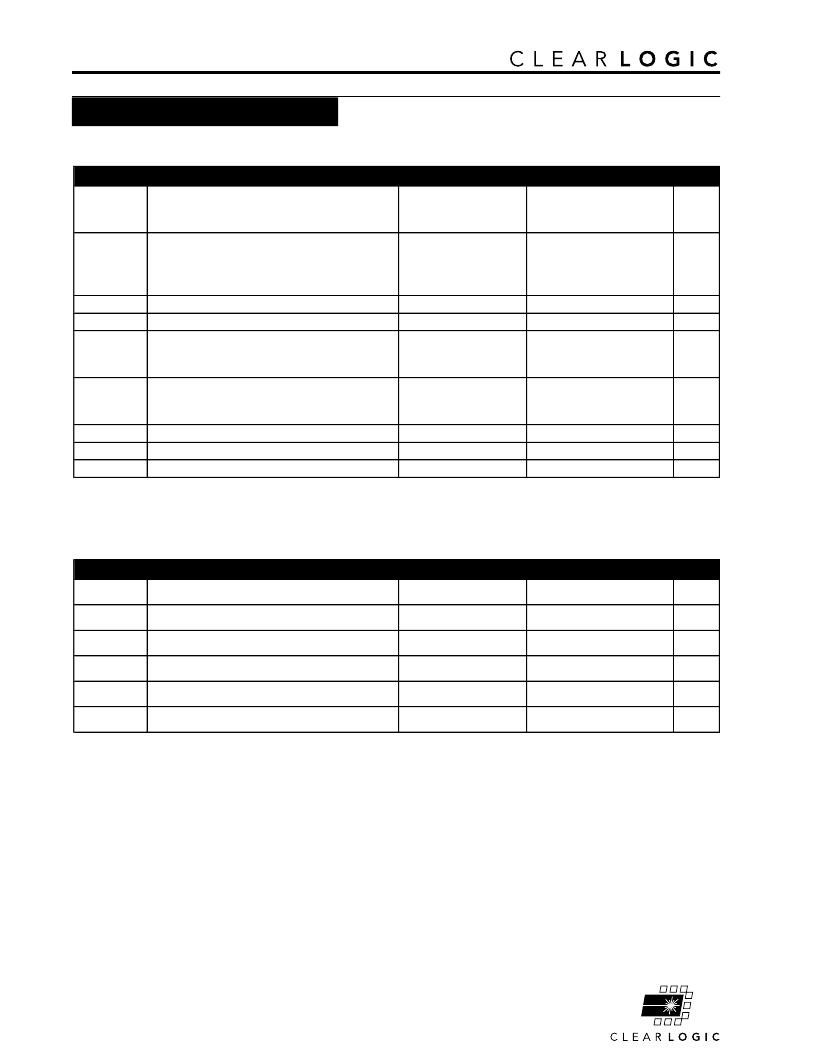
Absolute Maximum Ratings
Symbol
Recommended Operating Conditions
Symbol
Parameter
Supply voltage, internal logic and input buffers
Commercial Grade Devices
Industrial Grade Devices
DC input voltage
5.0 volt commercial
5.0 volt industrial
3.3 volt operation
V
I
Input voltage
V
O
Output voltage
Operating temperature
Commercial temperature range
Industrial temperature range
Junction Operating temperature
Commercial temperature range
Industrial temperature range
t
R
Input signal rise time
t
F
Input signal fall time
t
RVCC
V
CC
rise time
DC Electrical Specifications
Parameter
Conditions
Min
Max
Unit
CC
Supply voltage
With respect to ground
-2.0
7.0
V
V
I
DC input voltage
[1]
With respect to ground
-2.0
7.0
V
I
OUT
DC output current, per pin
-25
25
mA
T
STG
Storage temperature
No bias
-65
150
°C
T
AMB
Ambient temperature
Under bias
-65
135
°C
T
J
Junction temperature
Under bias
135
°C
7K tbl 03
Conditions
Min
Max
Unit
4.75
4.50
5.25
5.50
V
V
4.75
4.50
3.00
-0.5
0
5.25
3.60
V
V
V
V
V
V
CCINT
+0.5
V
CCIO
0
70
85
°C
°C
-40
0
90
105
40
40
100
°C
°C
ns
ns
ms
-40
V
CCINT
V
CCIO
T
A
7K tbl 02
T
J
相關(guān)PDF資料 |
PDF描述 |
|---|---|
| CL7192EQC160-12P | Laser-Programmable Complex PLD |
| CL7192EQC160-15 | |
| CL7192EQC160-20 | Laser-Programmable Complex PLD |
| CL7192EQI160-20 | |
| CL7192SQC160-10 | |
相關(guān)代理商/技術(shù)參數(shù) |
參數(shù)描述 |
|---|---|
| CL72001X | 制造商:BANDRIDGE 功能描述:LEAD AV CAT5 0.5M |
| CL72002X | 制造商:BANDRIDGE 功能描述:LEAD AV CAT5 2M |
| CL72003X | 制造商:BANDRIDGE 功能描述:LEAD AV CAT5 3M |
| CL72008X | 制造商:BANDRIDGE 功能描述:LEAD AV CAT5 7.5M |
| CL72015X | 制造商:BANDRIDGE 功能描述:LEAD AV CAT5 15M |
發(fā)布緊急采購(gòu),3分鐘左右您將得到回復(fù)。