- 您現(xiàn)在的位置:買賣IC網(wǎng) > PDF目錄384208 > CL7192EQC160-12 PDF資料下載
參數(shù)資料
| 型號: | CL7192EQC160-12 |
| 文件頁數(shù): | 13/16頁 |
| 文件大小: | 183K |
| 代理商: | CL7192EQC160-12 |
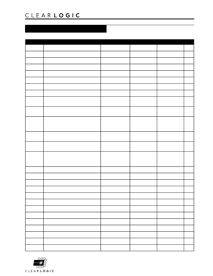
CL7192E and CL7192S Laser Processed Logic Devices
Page 13
Parameter
Conditions
Min
Max
Min
Max
Unit
t
iN
Input pad and buffer delay
2.0
3.0
ns
t
IO
I/O input pad and buffer delay
2.0
3.0
ns
t
FIN
Fast input delay
2.0
4.0
ns
t
SEXP
Shared expander delay
8.0
9.0
ns
t
PEXP
Parallel expander delay
1.0
2.0
ns
t
LAD
Logic array delay
6.0
8.0
ns
t
LAC
Logic control array delay
6.0
8.0
ns
t
IOE
Internal output enable delay
3.0
4.0
ns
Output buffer and pad delay
Slow slew rate = off, V
CCIO
= 5.0 V
Output buffer and pad delay
Slow slew rate = off, V
CCIO
= 3.3 V
Output buffer and pad delay
Slow slew rate = on,
V
CCIO
= 5.0 V or 3.3 V
Output buffer enable delay
Slow slew rate = off, V
CCIO
= 5.0 V
Output buffer enable delay
Slow slew rate = off, V
CCIO
= 3.3 V
Output buffer enable delay
Slow slew rate = on,
V
CCIO
= 5.0 V or 3.3 V
t
XZ
Output buffer disable delay
C
L
= 5 pF
[3]
6.0
10.0
ns
t
SU
Register setup time
4.0
4.0
ns
t
H
Register hold time
4.0
5.0
ns
t
FSU
Register setup time of fast input
2.0
4.0
ns
t
FH
Register hold time of fast input
1.0
3.0
ns
t
RD
Register delay
1.0
1.0
ns
t
COMB
Combinatorial delay
1.0
1.0
ns
t
IC
Array clock delay
6.0
8.0
ns
t
EN
Register enable time
6.0
8.0
ns
t
GLOB
Global control delay
1.0
3.0
ns
t
PRE
Register preset time
4.0
4.0
ns
t
CLR
Register clear time
4.0
4.0
ns
t
LIA
LIA delay
2.0
3.0
ns
Speed: -15
Speed: -20
Symbol
7K tbl 07D3
t
OD1
C
L
= 35 pF
4.0
5.0
ns
t
OD2
C
L
= 35 pF
5.0
6.0
ns
9.0
ns
t
OD3
C
L
= 35 pF
t
ZX1
C
L
= 35 pF
7.0
6.0
10.0
ns
11.0
ns
t
ZX2
C
L
= 35 pF
t
ZX3
C
L
= 35 pF
ns
7.0
10.0
14.0
AC Electrical Specifications cont.
Internal Timing Parameters
[4]
相關(guān)PDF資料 |
PDF描述 |
|---|---|
| CL7192EQC160-12P | Laser-Programmable Complex PLD |
| CL7192EQC160-15 | |
| CL7192EQC160-20 | Laser-Programmable Complex PLD |
| CL7192EQI160-20 | |
| CL7192SQC160-10 | |
相關(guān)代理商/技術(shù)參數(shù) |
參數(shù)描述 |
|---|---|
| CL72001X | 制造商:BANDRIDGE 功能描述:LEAD AV CAT5 0.5M |
| CL72002X | 制造商:BANDRIDGE 功能描述:LEAD AV CAT5 2M |
| CL72003X | 制造商:BANDRIDGE 功能描述:LEAD AV CAT5 3M |
| CL72008X | 制造商:BANDRIDGE 功能描述:LEAD AV CAT5 7.5M |
| CL72015X | 制造商:BANDRIDGE 功能描述:LEAD AV CAT5 15M |
發(fā)布緊急采購,3分鐘左右您將得到回復。