- 您現(xiàn)在的位置:買賣IC網(wǎng) > PDF目錄17092 > C8051F300-TB (Silicon Laboratories Inc)BOARD PROTOTYPING W/C8051F300 PDF資料下載
參數(shù)資料
| 型號: | C8051F300-TB |
| 廠商: | Silicon Laboratories Inc |
| 文件頁數(shù): | 127/178頁 |
| 文件大?。?/td> | 0K |
| 描述: | BOARD PROTOTYPING W/C8051F300 |
| 標(biāo)準(zhǔn)包裝: | 1 |
| 類型: | MCU |
| 適用于相關(guān)產(chǎn)品: | C8051F300 |
| 所含物品: | 板 |
第1頁第2頁第3頁第4頁第5頁第6頁第7頁第8頁第9頁第10頁第11頁第12頁第13頁第14頁第15頁第16頁第17頁第18頁第19頁第20頁第21頁第22頁第23頁第24頁第25頁第26頁第27頁第28頁第29頁第30頁第31頁第32頁第33頁第34頁第35頁第36頁第37頁第38頁第39頁第40頁第41頁第42頁第43頁第44頁第45頁第46頁第47頁第48頁第49頁第50頁第51頁第52頁第53頁第54頁第55頁第56頁第57頁第58頁第59頁第60頁第61頁第62頁第63頁第64頁第65頁第66頁第67頁第68頁第69頁第70頁第71頁第72頁第73頁第74頁第75頁第76頁第77頁第78頁第79頁第80頁第81頁第82頁第83頁第84頁第85頁第86頁第87頁第88頁第89頁第90頁第91頁第92頁第93頁第94頁第95頁第96頁第97頁第98頁第99頁第100頁第101頁第102頁第103頁第104頁第105頁第106頁第107頁第108頁第109頁第110頁第111頁第112頁第113頁第114頁第115頁第116頁第117頁第118頁第119頁第120頁第121頁第122頁第123頁第124頁第125頁第126頁當(dāng)前第127頁第128頁第129頁第130頁第131頁第132頁第133頁第134頁第135頁第136頁第137頁第138頁第139頁第140頁第141頁第142頁第143頁第144頁第145頁第146頁第147頁第148頁第149頁第150頁第151頁第152頁第153頁第154頁第155頁第156頁第157頁第158頁第159頁第160頁第161頁第162頁第163頁第164頁第165頁第166頁第167頁第168頁第169頁第170頁第171頁第172頁第173頁第174頁第175頁第176頁第177頁第178頁
C8051F300/1/2/3/4/5
52
Rev. 2.9
The output of Comparator0 can be polled in software, used as an interrupt source, and/or routed to a Port
pin. When routed to a Port pin, the Comparator0 output is available asynchronous or synchronous to the
system clock; the asynchronous output is available even in STOP mode (with no system clock active).
When disabled, the Comparator0 output (if assigned to a Port I/O pin via the Crossbar) defaults to the logic
low state, and its supply current falls to less than 100 nA. See Section “12.1. Priority Crossbar
Decoder” on page 104 for details on configuring the Comparator0 output via the digital Crossbar.
Comparator0 inputs can be externally driven from –0.25 to (VDD) + 0.25 V without damage or upset. The
complete electrical specifications for Comparator0 are given in Table 7.1.
The Comparator0 response time may be configured in software via the CP0MD1-0 bits in register
CPT0MD (see SFR Definition 7.3). Selecting a longer response time reduces the amount of power con-
sumed by Comparator0. See Table 7.1 for complete timing and power consumption specifications.
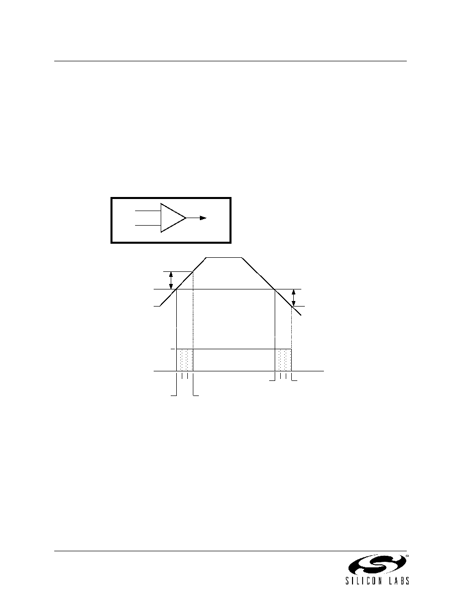
Positive Hysteresis Voltage
(Programmed with CP0HYP Bits)
Negative Hysteresis Voltage
(Programmed by CP0HYN Bits)
VIN-
VIN+
INPUTS
CIRCUIT CONFIGURATION
+
_
CP0+
CP0-
CP0
VIN+
VIN-
OUT
VOH
Positive Hysteresis
Disabled
Maximum
Positive Hysteresis
Negative Hysteresis
Disabled
Maximum
Negative Hysteresis
OUTPUT
VOL
Figure 7.2. Comparator Hysteresis Plot
The hysteresis of Comparator0 is software-programmable via its Comparator0 Control register (CPT0CN).
The user can program both the amount of hysteresis voltage (referred to the input voltage) and the positive
and negative-going symmetry of this hysteresis around the threshold voltage.
The Comparator0 hysteresis is programmed using Bits3–0 in the Comparator0 Control Register CPT0CN
(shown in SFR Definition 7.1). The amount of negative hysteresis voltage is determined by the settings of
the CP0HYN bits. As shown in Figure 7.2, settings of 20, 10 or 5 mV of negative hysteresis can be pro-
grammed, or negative hysteresis can be disabled. In a similar way, the amount of positive hysteresis is
determined by the setting the CP0HYP bits.
相關(guān)PDF資料 |
PDF描述 |
|---|---|
| 0210391037 | CABLE JUMPER 1MM .102M 33POS |
| C8051F226-TB | BOARD PROTOTYPING W/C8051F226 |
| C8051F330-TB | BOARD PROTOTYPING W/C8051F330 |
| LGU2G101MELA | CAP ALUM 100UF 400V 20% SNAP |
| SDR-Q | SCOTCH CODE REFILL Q |
相關(guān)代理商/技術(shù)參數(shù) |
參數(shù)描述 |
|---|---|
| C8051F300-TB-K | 功能描述:BOARD PROTOTYPING W/C8051F300 制造商:silicon labs 系列:- 零件狀態(tài):在售 板類型:評估平臺 類型:MCU 8-位 核心處理器:8051 操作系統(tǒng):- 平臺:- 配套使用產(chǎn)品/相關(guān)產(chǎn)品:C8051F30x 安裝類型:固定 內(nèi)容:板 標(biāo)準(zhǔn)包裝:1 |
| C8051F301 | 功能描述:8位微控制器 -MCU 8KB 2%osc RoHS:否 制造商:Silicon Labs 核心:8051 處理器系列:C8051F39x 數(shù)據(jù)總線寬度:8 bit 最大時鐘頻率:50 MHz 程序存儲器大小:16 KB 數(shù)據(jù) RAM 大小:1 KB 片上 ADC:Yes 工作電源電壓:1.8 V to 3.6 V 工作溫度范圍:- 40 C to + 105 C 封裝 / 箱體:QFN-20 安裝風(fēng)格:SMD/SMT |
| C8051F301-GM | 功能描述:8位微控制器 -MCU 8KB 11P MCU RoHS:否 制造商:Silicon Labs 核心:8051 處理器系列:C8051F39x 數(shù)據(jù)總線寬度:8 bit 最大時鐘頻率:50 MHz 程序存儲器大小:16 KB 數(shù)據(jù) RAM 大小:1 KB 片上 ADC:Yes 工作電源電壓:1.8 V to 3.6 V 工作溫度范圍:- 40 C to + 105 C 封裝 / 箱體:QFN-20 安裝風(fēng)格:SMD/SMT |
| C8051F301-GMR | 功能描述:8位微控制器 -MCU 8KB 11P MCU RoHS:否 制造商:Silicon Labs 核心:8051 處理器系列:C8051F39x 數(shù)據(jù)總線寬度:8 bit 最大時鐘頻率:50 MHz 程序存儲器大小:16 KB 數(shù)據(jù) RAM 大小:1 KB 片上 ADC:Yes 工作電源電壓:1.8 V to 3.6 V 工作溫度范圍:- 40 C to + 105 C 封裝 / 箱體:QFN-20 安裝風(fēng)格:SMD/SMT |
| C8051F301-GS | 功能描述:8位微控制器 -MCU 8KB Flash 2%osc RoHS:否 制造商:Silicon Labs 核心:8051 處理器系列:C8051F39x 數(shù)據(jù)總線寬度:8 bit 最大時鐘頻率:50 MHz 程序存儲器大小:16 KB 數(shù)據(jù) RAM 大小:1 KB 片上 ADC:Yes 工作電源電壓:1.8 V to 3.6 V 工作溫度范圍:- 40 C to + 105 C 封裝 / 箱體:QFN-20 安裝風(fēng)格:SMD/SMT |
發(fā)布緊急采購,3分鐘左右您將得到回復(fù)。