- 您現(xiàn)在的位置:買賣IC網(wǎng) > PDF目錄22090 > ATF1508BE-7AU100 (Atmel)IC CPLD 128MC 1.8V ISP 100TQFP PDF資料下載
參數(shù)資料
| 型號(hào): | ATF1508BE-7AU100 |
| 廠商: | Atmel |
| 文件頁數(shù): | 5/30頁 |
| 文件大?。?/td> | 0K |
| 描述: | IC CPLD 128MC 1.8V ISP 100TQFP |
| 標(biāo)準(zhǔn)包裝: | 90 |
| 系列: | ATF15xx |
| 可編程類型: | 系統(tǒng)內(nèi)可編程(最少 10,000 次編程/擦除循環(huán)) |
| 最大延遲時(shí)間 tpd(1): | 7.5ns |
| 電壓電源 - 內(nèi)部: | 1.7 V ~ 1.9 V |
| 宏單元數(shù): | 128 |
| 輸入/輸出數(shù): | 80 |
| 工作溫度: | -40°C ~ 85°C |
| 安裝類型: | 表面貼裝 |
| 封裝/外殼: | 100-TQFP |
| 供應(yīng)商設(shè)備封裝: | 100-TQFP(14x14) |
| 包裝: | 托盤 |
第1頁第2頁第3頁第4頁當(dāng)前第5頁第6頁第7頁第8頁第9頁第10頁第11頁第12頁第13頁第14頁第15頁第16頁第17頁第18頁第19頁第20頁第21頁第22頁第23頁第24頁第25頁第26頁第27頁第28頁第29頁第30頁
13
3663A–PLD–1/08
ATF1508BE
6.
JTAG-BST/ISP Overview
The JTAG boundary-scan testing is controlled by the Test Access Port (TAP) controller in the
ATF1508BE. The boundary-scan technique involves the inclusion of a shift-register stage (con-
tained in a boundary-scan cell) adjacent to each component so that signals at component
boundaries can be controlled and observed using scan testing methods. Each input pin and I/O
pin has its own boundary-scan cell (BSC) to support boundary-scan testing. The TAP controller
is automatically reset at power-up. The five JTAG modes supported include: SAMPLE/PRE-
LOAD, EXTEST, BYPASS, IDCODE and HIGHZ. The ATF1508BE’s BSC can be fully described
using a BSDL file as described in IEEE 1149.1 standard. This allows ATF1508BE testing to be
described and implemented using any one of the third-party development tools supporting this
standard.
The ATF1508BE also has the option of using the four JTAG-standard I/O pins for ISP. The
ATF1508BE is programmable through the four JTAG pins using the IEEE standard JTAG pro-
gramming protocol established by IEEE 1532 standard using 1.8V/2.5V/3.3V LVCMOS level
programming signals from the ISP interface for in-system programming. The JTAG feature is a
programmable option. If JTAG (BST or ISP) is not needed, then the four JTAG control pins are
available as I/O pins.
6.1
JTAG Boundary-scan Cell (BSC) Testing
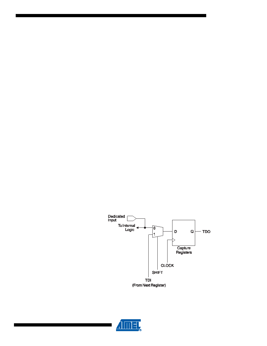
The ATF1508BE contains 80 I/O pins and four dedicated input pins. Each input pin and I/O pin
has its own boundary-scan cell (BSC) in order to support boundary-scan testing as described in
detail by IEEE 1532 standard. A typical BSC consists of three capture registers or scan registers
and up to two update registers. There are two types of BSCs, one for input or I/O pin, and one
for the macrocells. The BSCs in the device are chained together through the capture registers.
Input to the capture register chain is fed in from the TDI pin while the output is directed to the
TDO pin. Capture registers are used to capture active device data signals, to shift data in and
out of the device and to load data into the update registers. Control signals are generated inter-
nally by the JTAG TAP controller. The BSC configuration for the input and I/O pins and
macrocells is shown below.
Figure 6-1.
BSC Configuration for Input and I/O Pins (Except JTAG TAP Pins)
Note:
The ATF1508BE has a pull-up option on TMS and TDI pins. This feature is selected as a design
option.
相關(guān)PDF資料 |
PDF描述 |
|---|---|
| GSA43DTBT | CONN EDGECARD 86POS R/A .125 SLD |
| M4A3-96/48-10VC | IC CPLD ISP 4A 96MC 100TQFP |
| 5145427-5 | SEC-Z CONN ASSY 60 QUAD POS LF |
| GRM31A7U3A101JW31D | CAP CER 100PF 1KV 5% U2J 1206 |
| LC4064V-75T48I | IC PLD 64MC 32I/O 7.5NS 48TQFP |
相關(guān)代理商/技術(shù)參數(shù) |
參數(shù)描述 |
|---|---|
| ATF1508BE-7CU132 | 制造商:ATMEL 制造商全稱:ATMEL Corporation 功能描述:Highperformance CPLD |
| ATF1508JC68-10 | 制造商:未知廠家 制造商全稱:未知廠家 功能描述:Flash Complex PLD |
| ATF1508JC68-15 | 制造商:未知廠家 制造商全稱:未知廠家 功能描述:Flash Complex PLD |
| ATF1508JC68-7 | 制造商:未知廠家 制造商全稱:未知廠家 功能描述:Flash Complex PLD |
| ATF1508JC84-10 | 制造商:未知廠家 制造商全稱:未知廠家 功能描述:Flash Complex PLD |
發(fā)布緊急采購,3分鐘左右您將得到回復(fù)。