- 您現(xiàn)在的位置:買賣IC網(wǎng) > PDF目錄4432 > APA300-FG256I (Microsemi SoC)IC FPGA PROASIC+ 300K 256-FBGA PDF資料下載
參數(shù)資料
| 型號(hào): | APA300-FG256I |
| 廠商: | Microsemi SoC |
| 文件頁(yè)數(shù): | 93/178頁(yè) |
| 文件大?。?/td> | 0K |
| 描述: | IC FPGA PROASIC+ 300K 256-FBGA |
| 標(biāo)準(zhǔn)包裝: | 90 |
| 系列: | ProASICPLUS |
| RAM 位總計(jì): | 73728 |
| 輸入/輸出數(shù): | 186 |
| 門數(shù): | 300000 |
| 電源電壓: | 2.3 V ~ 2.7 V |
| 安裝類型: | 表面貼裝 |
| 工作溫度: | -40°C ~ 85°C |
| 封裝/外殼: | 256-LBGA |
| 供應(yīng)商設(shè)備封裝: | 256-FPBGA(17x17) |
第1頁(yè)第2頁(yè)第3頁(yè)第4頁(yè)第5頁(yè)第6頁(yè)第7頁(yè)第8頁(yè)第9頁(yè)第10頁(yè)第11頁(yè)第12頁(yè)第13頁(yè)第14頁(yè)第15頁(yè)第16頁(yè)第17頁(yè)第18頁(yè)第19頁(yè)第20頁(yè)第21頁(yè)第22頁(yè)第23頁(yè)第24頁(yè)第25頁(yè)第26頁(yè)第27頁(yè)第28頁(yè)第29頁(yè)第30頁(yè)第31頁(yè)第32頁(yè)第33頁(yè)第34頁(yè)第35頁(yè)第36頁(yè)第37頁(yè)第38頁(yè)第39頁(yè)第40頁(yè)第41頁(yè)第42頁(yè)第43頁(yè)第44頁(yè)第45頁(yè)第46頁(yè)第47頁(yè)第48頁(yè)第49頁(yè)第50頁(yè)第51頁(yè)第52頁(yè)第53頁(yè)第54頁(yè)第55頁(yè)第56頁(yè)第57頁(yè)第58頁(yè)第59頁(yè)第60頁(yè)第61頁(yè)第62頁(yè)第63頁(yè)第64頁(yè)第65頁(yè)第66頁(yè)第67頁(yè)第68頁(yè)第69頁(yè)第70頁(yè)第71頁(yè)第72頁(yè)第73頁(yè)第74頁(yè)第75頁(yè)第76頁(yè)第77頁(yè)第78頁(yè)第79頁(yè)第80頁(yè)第81頁(yè)第82頁(yè)第83頁(yè)第84頁(yè)第85頁(yè)第86頁(yè)第87頁(yè)第88頁(yè)第89頁(yè)第90頁(yè)第91頁(yè)第92頁(yè)當(dāng)前第93頁(yè)第94頁(yè)第95頁(yè)第96頁(yè)第97頁(yè)第98頁(yè)第99頁(yè)第100頁(yè)第101頁(yè)第102頁(yè)第103頁(yè)第104頁(yè)第105頁(yè)第106頁(yè)第107頁(yè)第108頁(yè)第109頁(yè)第110頁(yè)第111頁(yè)第112頁(yè)第113頁(yè)第114頁(yè)第115頁(yè)第116頁(yè)第117頁(yè)第118頁(yè)第119頁(yè)第120頁(yè)第121頁(yè)第122頁(yè)第123頁(yè)第124頁(yè)第125頁(yè)第126頁(yè)第127頁(yè)第128頁(yè)第129頁(yè)第130頁(yè)第131頁(yè)第132頁(yè)第133頁(yè)第134頁(yè)第135頁(yè)第136頁(yè)第137頁(yè)第138頁(yè)第139頁(yè)第140頁(yè)第141頁(yè)第142頁(yè)第143頁(yè)第144頁(yè)第145頁(yè)第146頁(yè)第147頁(yè)第148頁(yè)第149頁(yè)第150頁(yè)第151頁(yè)第152頁(yè)第153頁(yè)第154頁(yè)第155頁(yè)第156頁(yè)第157頁(yè)第158頁(yè)第159頁(yè)第160頁(yè)第161頁(yè)第162頁(yè)第163頁(yè)第164頁(yè)第165頁(yè)第166頁(yè)第167頁(yè)第168頁(yè)第169頁(yè)第170頁(yè)第171頁(yè)第172頁(yè)第173頁(yè)第174頁(yè)第175頁(yè)第176頁(yè)第177頁(yè)第178頁(yè)
ProASICPLUS Flash Family FPGAs
v5.9
2-11
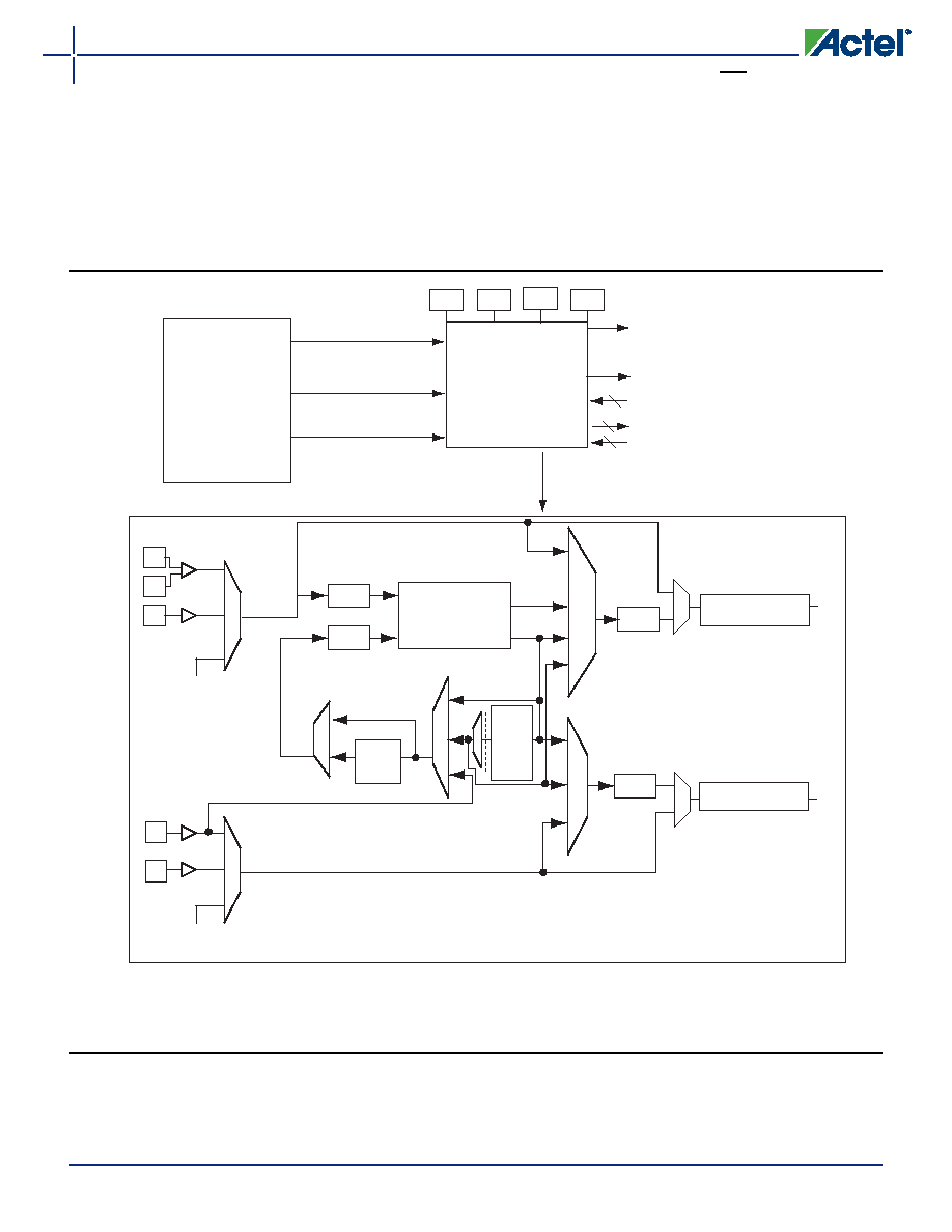
The clock conditioning circuit can advance or delay the
clock up to 8 ns (in increments of 0.25 ns) relative to the
positive edge of the incoming reference clock. The system
also allows for the selection of output frequency clock
phases of 0° and 180°.
Prior to the application of signals to the rib drivers, they
pass through programmable delay units, one per global
network. These units permit the delaying of global
signals relative to other signals to assist in the control of
input set-up times. Not all possible combinations of input
and output modes can be used. The degrees of freedom
available in the bidirectional global pad system and in
the clock conditioning circuit have been restricted. This
avoids unnecessary and unwieldy design kit and software
work.
Notes:
1. FBDLY is a programmable delay line from 0 to 4 ns in 250 ps increments.
2. DLYA and DLYB are programmable delay lines, each with selectable values 0 ps, 250 ps, 500 ps, and 4 ns.
3. OBDIV will also divide the phase-shift since it takes place after the PLL Core.
Figure 2-11 PLL Block – Top-Level View and Detailed PLL Block Diagram
AVDD
AGND
GND
+
-
VDD
External Feedback Signal
GLA
GLB
Dynamic
Configuration Bits
Flash
Configuration Bits
8
27
4
Clock Conditioning
Circuitry
(Top level view)
Global MUX A OUT
Global MUX B OUT
See Figure 2-15
on page 2-15
Input Pins to the PLL
GLB
GLA
÷u
÷v
PLL Core
0°
180°
0
1
6
7
5
4
2
Delay Line 0.0 ns, 0.25 ns,
0.50 ns and 4.00 ns
P+
P-
Clock from Core
(GLINT mode)
CLK
1
0
Deskew
Delay
2.95 ns
1
2
3
Delay Line
0.25 ns to
4.00 ns,
16 steps,
0.25 ns
increments
3
1
2
Delay Line 0.0 ns, 0.25 ns,
0.50 ns and 4.00 ns
Clock from Core
(GLINT mode)
CLKA
EXTFB
XDLYSEL
Bypass Secondary
Bypass Primary
FIVDIV[4:0]
FBDIV[5:0]
FBSEL[1:0]
OAMUX[1:0]
DLYA[1:0]
DLYB[1:0]
OBDIV[1:0]
OBMUX[2:0]
OADIV[1:0]
FBDLY[3:0]
÷n
÷m
Clock Conditioning Circuitry Detailed Block Diagram
相關(guān)PDF資料 |
PDF描述 |
|---|---|
| APA300-FGG256I | IC FPGA PROASIC+ 300K 256-FBGA |
| A54SX16P-TQ176I | IC FPGA SX 24K GATES 176-TQFP |
| A54SX16P-1TQ176 | IC FPGA SX 24K GATES 176-TQFP |
| HMM44DRYF | CONN EDGECARD 88POS DIP .156 SLD |
| AMM25DRMN | CONN EDGECARD 50POS .156 WW |
相關(guān)代理商/技術(shù)參數(shù) |
參數(shù)描述 |
|---|---|
| APA300-FG256M | 制造商:Microsemi Corporation 功能描述:FPGA ProASICPLUS Family 300K Gates 180MHz 0.22um (CMOS) Technology 2.5V 256-Pin FBGA 制造商:Microsemi SOC Products Group 功能描述:FPGA PROASICPLUS FAMILY 300K GATES 180MHZ 0.22UM (CMOS) TECH - Trays |
| APA300-FG896A | 制造商:ACTEL 制造商全稱:Actel Corporation 功能描述:Automotive-Grade ProASIC Flash Family FPGAs |
| APA300-FGB | 制造商:ACTEL 制造商全稱:Actel Corporation 功能描述:ProASIC Flash Family FPGAs |
| APA300-FGES | 制造商:ACTEL 制造商全稱:Actel Corporation 功能描述:ProASIC Flash Family FPGAs |
| APA300-FGG144 | 功能描述:IC FPGA PROASIC+ 300K 144-FBGA RoHS:是 類別:集成電路 (IC) >> 嵌入式 - FPGA(現(xiàn)場(chǎng)可編程門陣列) 系列:ProASICPLUS 標(biāo)準(zhǔn)包裝:40 系列:SX-A LAB/CLB數(shù):6036 邏輯元件/單元數(shù):- RAM 位總計(jì):- 輸入/輸出數(shù):360 門數(shù):108000 電源電壓:2.25 V ~ 5.25 V 安裝類型:表面貼裝 工作溫度:0°C ~ 70°C 封裝/外殼:484-BGA 供應(yīng)商設(shè)備封裝:484-FPBGA(27X27) |
發(fā)布緊急采購(gòu),3分鐘左右您將得到回復(fù)。