- 您現(xiàn)在的位置:買賣IC網(wǎng) > PDF目錄357602 > AP7168-SPG-13 (DIODES INC) 0.8 V-5 V ADJUSTABLE POSITIVE LDO REGULATOR, 0.8 V DROPOUT, PDSO8 PDF資料下載
參數(shù)資料
| 型號(hào): | AP7168-SPG-13 |
| 廠商: | DIODES INC |
| 元件分類: | 可調(diào)正電壓單路輸出LDO穩(wěn)壓器 |
| 英文描述: | 0.8 V-5 V ADJUSTABLE POSITIVE LDO REGULATOR, 0.8 V DROPOUT, PDSO8 |
| 封裝: | GREEN, SOP-8 |
| 文件頁數(shù): | 7/11頁 |
| 文件大小: | 461K |
| 代理商: | AP7168-SPG-13 |
AP7168
1.2A LOW DROPOUT REGULATOR WITH POK
AP7168
Document number: DS32019 Rev. 2 - 2
7 of 11
September 2010 Diodes Incorporated
N
Typical Performance Characteristics
(Continued)
Current Limit vs. Temperature
1.4
1.5
1.6
1.7
1.8
-50
-25
0
Temperature (
o
C)
25
50
75
100
C
VIN =2.8V,Vout=1.8V
VIN =3.3V,Vout=1.8V
Application Note
Input Capacitor
A 1
μ
F ceramic capacitor is recommended to connect
between IN and GND pins to decouple input power supply
glitch and noise. The amount of the capacitance may be
increased without limit. A lower ESR (Equivalent Series
Resistance) capacitor allows the use of less capacitance,
while higher ESR type requires more capacitance. This
input capacitor should be located as close as possible to
the device to assure input stability and less noise. For
PCB layout, a wide copper trace is required for both IN
and GND.
Output Capacitor
The output capacitor is required to stabilize and help the
transient response of the LDO. The AP7168 is designed to
have excellent transient response for most applications
with a small amount of output capacitance. The AP7168 is
stable for all available types and values of output
capacitors
≥
4.7
μ
F. The device is also stable with multiple
capacitors in parallel, which can be of any type of value.
Additional capacitance helps to reduce undershoot and
overshoot during transient. This capacitor should be
placed as close as possible to OUT and GND pins for
optimum performance.
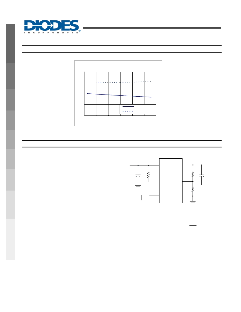
Adjustable Operation
The AP7168 provides output voltage from 0.8V to 5.0V
through external resistor divider as shown below.
IN
GND
EN
OUT
Enable
FB
V
IN
V
OUT
POK
100kOhm
R
1
R
2
AP7168
C
IN
C
OUT
The output voltage is calculated by:
+
=
2
1
REF
V
OUT
V
R
R
1
Where V
REF
=0.8V (the internal reference voltage)
Rearranging the equation will give the following equation
to find the approximate resistor divider values:
=
V
1
V
R
R
REF
OUT
2
1
To maintain the stability of the internal reference voltage,
R
2
needs to be kept smaller than 250k
Ω
.
相關(guān)PDF資料 |
PDF描述 |
|---|---|
| AP7312-1525W6-7 | FIXED POSITIVE LDO REGULATOR, PDSO6 |
| AP7312-1525FM-7 | FIXED POSITIVE LDO REGULATOR, PDSO6 |
| AP8800M8G-13 | |
| AP8800FNG-7 | |
| AP8800SG-13 | |
相關(guān)代理商/技術(shù)參數(shù) |
參數(shù)描述 |
|---|---|
| AP7-1-69-103 | 制造商:Sensata Technologies 功能描述:Circuit Breaker Magnetic 1Pole 10A |
| AP7-1-69-153 | 制造商:Sensata Technologies 功能描述:Circuit Breaker Magnetic Circuit Protectors 1Pole 15A 240VAC |
| AP7-1-69-203 | 制造商:Sensata Technologies 功能描述:Circuit Breaker Magnetic Circuit Protectors 1Pole 20A 240VAC |
| AP7-1-69-251 | 制造商:Sensata Technologies 功能描述:Circuit Breaker Magnetic 1Pole 0.25A |
| AP7-1-69-252 | 制造商:Sensata Technologies 功能描述:Circuit Breaker Magnetic 1Pole 2.5A 240VAC/50VDC |
發(fā)布緊急采購,3分鐘左右您將得到回復(fù)。