- 您現(xiàn)在的位置:買賣IC網(wǎng) > PDF目錄57938 > AO4813 (ALPHA AND OMEGA SEMICONDUCTOR) 7100 mA, 30 V, 2 CHANNEL, P-CHANNEL, Si, SMALL SIGNAL, MOSFET PDF資料下載
參數(shù)資料
| 型號: | AO4813 |
| 廠商: | ALPHA AND OMEGA SEMICONDUCTOR |
| 元件分類: | 小信號晶體管 |
| 英文描述: | 7100 mA, 30 V, 2 CHANNEL, P-CHANNEL, Si, SMALL SIGNAL, MOSFET |
| 封裝: | GREEN, SOIC-8 |
| 文件頁數(shù): | 6/6頁 |
| 文件大?。?/td> | 280K |
| 代理商: | AO4813 |
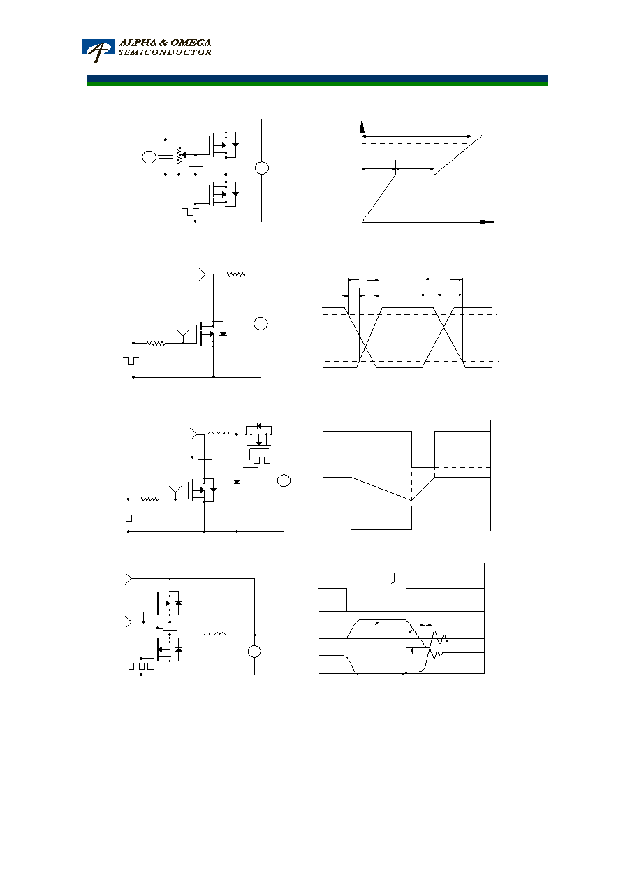
AO4813
VDC
Ig
Vds
DUT
VDC
Vgs
Qg
Qgs
Qgd
Charge
Gate Charge Test Circuit & Waveform
-
+
-
+
-10V
Vdd
Vgs
Id
Vgs
Rg
DUT
VDC
Vgs
Vds
Id
Vgs
Unclamped Inductive Switching (UIS) Test Circuit & Waveforms
Vds
L
-
+
2
E
= 1/2 LI
AR
BV
DSS
I AR
Ig
Vgs
-
+
VDC
DUT
L
Vgs
Isd
Diode Recovery Test Circuit & Waveforms
Vds -
Vds +
dI/dt
RM
rr
Vdd
Q
= - Idt
t
rr
-Isd
-Vds
F
-I
VDC
DUT
Vdd
Vgs
Vds
Vgs
RL
Rg
Resistive Switching Test Circuit & Waveforms
-
+
Vgs
Vds
t
90%
10%
r
on
d(off)
f
off
d(on)
Rev 9: April 2011
www.aosmd.com
Page 6 of 6
發(fā)布緊急采購,3分鐘左右您將得到回復(fù)。