- 您現(xiàn)在的位置:買賣IC網(wǎng) > PDF目錄375310 > AM70PDL127BDH66IS (SPANSION LLC) 2 x 64 Megabit (8 M x 16-Bit) CMOS 3.0 Volt-Only Page Mode Flash Memory Data Storage 128 Megabit (8 M x 16-Bit) CMOS PDF資料下載
參數(shù)資料
| 型號(hào): | AM70PDL127BDH66IS |
| 廠商: | SPANSION LLC |
| 元件分類: | 存儲(chǔ)器 |
| 英文描述: | 2 x 64 Megabit (8 M x 16-Bit) CMOS 3.0 Volt-Only Page Mode Flash Memory Data Storage 128 Megabit (8 M x 16-Bit) CMOS |
| 中文描述: | SPECIALTY MEMORY CIRCUIT, PBGA93 |
| 封裝: | 13 X 9 MM, FBGA-93 |
| 文件頁(yè)數(shù): | 57/128頁(yè) |
| 文件大小: | 918K |
| 代理商: | AM70PDL127BDH66IS |
第1頁(yè)第2頁(yè)第3頁(yè)第4頁(yè)第5頁(yè)第6頁(yè)第7頁(yè)第8頁(yè)第9頁(yè)第10頁(yè)第11頁(yè)第12頁(yè)第13頁(yè)第14頁(yè)第15頁(yè)第16頁(yè)第17頁(yè)第18頁(yè)第19頁(yè)第20頁(yè)第21頁(yè)第22頁(yè)第23頁(yè)第24頁(yè)第25頁(yè)第26頁(yè)第27頁(yè)第28頁(yè)第29頁(yè)第30頁(yè)第31頁(yè)第32頁(yè)第33頁(yè)第34頁(yè)第35頁(yè)第36頁(yè)第37頁(yè)第38頁(yè)第39頁(yè)第40頁(yè)第41頁(yè)第42頁(yè)第43頁(yè)第44頁(yè)第45頁(yè)第46頁(yè)第47頁(yè)第48頁(yè)第49頁(yè)第50頁(yè)第51頁(yè)第52頁(yè)第53頁(yè)第54頁(yè)第55頁(yè)第56頁(yè)當(dāng)前第57頁(yè)第58頁(yè)第59頁(yè)第60頁(yè)第61頁(yè)第62頁(yè)第63頁(yè)第64頁(yè)第65頁(yè)第66頁(yè)第67頁(yè)第68頁(yè)第69頁(yè)第70頁(yè)第71頁(yè)第72頁(yè)第73頁(yè)第74頁(yè)第75頁(yè)第76頁(yè)第77頁(yè)第78頁(yè)第79頁(yè)第80頁(yè)第81頁(yè)第82頁(yè)第83頁(yè)第84頁(yè)第85頁(yè)第86頁(yè)第87頁(yè)第88頁(yè)第89頁(yè)第90頁(yè)第91頁(yè)第92頁(yè)第93頁(yè)第94頁(yè)第95頁(yè)第96頁(yè)第97頁(yè)第98頁(yè)第99頁(yè)第100頁(yè)第101頁(yè)第102頁(yè)第103頁(yè)第104頁(yè)第105頁(yè)第106頁(yè)第107頁(yè)第108頁(yè)第109頁(yè)第110頁(yè)第111頁(yè)第112頁(yè)第113頁(yè)第114頁(yè)第115頁(yè)第116頁(yè)第117頁(yè)第118頁(yè)第119頁(yè)第120頁(yè)第121頁(yè)第122頁(yè)第123頁(yè)第124頁(yè)第125頁(yè)第126頁(yè)第127頁(yè)第128頁(yè)
November 25, 2003
Am70PDL127BDH/Am70PDL129BDH
55
A D V A N C E I N F O R M A T I O N
RY/BY#: Ready/Busy#
The RY/BY# is a dedicated, open-drain output pin
which indicates whether an Embedded Algorithm is in
progress or complete. The RY/BY# status is valid after
the rising edge of the final WE# pulse in the command
sequence. Since RY/BY# is an open-drain output, sev-
eral RY/BY# pins can be tied together in parallel with a
pull-up resistor to V
CC
.
If the output is low (Busy), the device is actively eras-
ing or programming. (This includes programming in
the Erase Suspend mode.) If the output is high
(Ready), the device is in the read mode, the standby
mode, or one of the banks is in the erase-sus-
pend-read mode.
Table 18 shows the outputs for RY/BY#.
DQ6: Toggle Bit I
Toggle Bit I on DQ6 indicates whether an Embedded
Program or Erase algorithm is in progress or com-
plete, or whether the device has entered the Erase
Suspend mode. Toggle Bit I may be read at any ad-
dress, and is valid after the rising edge of the final
WE# pulse in the command sequence (prior to the
program or erase operation), and during the sector
erase time-out.
During an Embedded Program or Erase algorithm op-
eration, successive read cycles to any address cause
DQ6 to toggle. The system may use either OE# or
CE#f1 to control the read cycles. When the operation
is complete, DQ6 stops toggling.
After an erase command sequence is written, if all
sectors selected for erasing are protected, DQ6 tog-
gles for approximately 400 μs, then returns to reading
array data. If not all selected sectors are protected, the
Embedded Erase algorithm erases the unprotected
sectors, and ignores the selected sectors that are pro-
tected.
The system can use DQ6 and DQ2 together to deter-
mine whether a sector is actively erasing or is
erase-suspended. When the device is actively erasing
(that is, the Embedded Erase algorithm is in progress),
DQ6 toggles. When the device enters the Erase Sus-
pend mode, DQ6 stops toggling. However, the system
must also use DQ2 to determine which sectors are
erasing or erase-suspended. Alternatively, the system
can use DQ7 (see the subsection on DQ7: Data# Poll-
ing).
If a program address falls within a protected sector,
DQ6 toggles for approximately 1 μs after the program
command sequence is written, then returns to reading
array data.
DQ6 also toggles during the erase-suspend-program
mode, and stops toggling once the Embedded Pro-
gram algorithm is complete.
Table 18 shows the outputs for Toggle Bit I on DQ6.
Figure 6 shows the toggle bit algorithm.
Figure 17
in
the
“Flash AC Characteristics”
section shows the tog-
gle bit timing diagrams. Figure 18 shows the differ-
ences between DQ2 and DQ6 in graphical form. See
also the subsection on DQ2: Toggle Bit II.
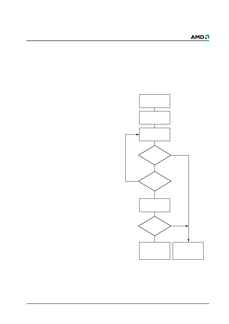
Figure 7.
Toggle Bit Algorithm
START
No
Yes
Yes
DQ5 = 1
No
Yes
Toggle Bit
= Toggle
No
Program/Erase
Operation Not
Complete, Write
Reset Command
Program/Erase
Operation Complete
Toggle Bit
= Toggle
Read Byte Twice
(DQ7–DQ0)
Address = VA
Read Byte
(DQ7–DQ0)
Address =VA
Read Byte
(DQ7–DQ0)
Address =VA
Note:
The system should recheck the toggle bit even if DQ5
= “1” because the toggle bit may stop toggling as DQ5
changes to “1.” See the subsections on DQ6 and DQ2 for
more information.
相關(guān)PDF資料 |
PDF描述 |
|---|---|
| AM70PDL127BDH66IT | 2 x 64 Megabit (8 M x 16-Bit) CMOS 3.0 Volt-Only Page Mode Flash Memory Data Storage 128 Megabit (8 M x 16-Bit) CMOS |
| AM70PDL127BDH85IS | 2 x 64 Megabit (8 M x 16-Bit) CMOS 3.0 Volt-Only Page Mode Flash Memory Data Storage 128 Megabit (8 M x 16-Bit) CMOS |
| AM70PDL129BDH | 2 x 64 Megabit (8 M x 16-Bit) CMOS 3.0 Volt-Only Page Mode Flash Memory Data Storage 128 Megabit (8 M x 16-Bit) CMOS |
| AM70PDL129BDH66IS | 2 x 64 Megabit (8 M x 16-Bit) CMOS 3.0 Volt-Only Page Mode Flash Memory Data Storage 128 Megabit (8 M x 16-Bit) CMOS |
| AM70PDL129BDH66IT | 2 x 64 Megabit (8 M x 16-Bit) CMOS 3.0 Volt-Only Page Mode Flash Memory Data Storage 128 Megabit (8 M x 16-Bit) CMOS |
相關(guān)代理商/技術(shù)參數(shù) |
參數(shù)描述 |
|---|---|
| AM70PDL127BDH66IT | 制造商:SPANSION 制造商全稱:SPANSION 功能描述:2 x 64 Megabit (8 M x 16-Bit) CMOS 3.0 Volt-Only Page Mode Flash Memory Data Storage 128 Megabit (8 M x 16-Bit) CMOS |
| AM70PDL127BDH85I | 制造商:SPANSION 制造商全稱:SPANSION 功能描述:Stacked Multi-Chip Package (MCP/XIP) Flash Memory, Data storage MirrorBit Flash, and pSRAM (XIP) |
| AM70PDL127BDH85IS | 制造商:SPANSION 制造商全稱:SPANSION 功能描述:2 x 64 Megabit (8 M x 16-Bit) CMOS 3.0 Volt-Only Page Mode Flash Memory Data Storage 128 Megabit (8 M x 16-Bit) CMOS |
| AM70PDL127BDH85IT | 制造商:SPANSION 制造商全稱:SPANSION 功能描述:2 x 64 Megabit (8 M x 16-Bit) CMOS 3.0 Volt-Only Page Mode Flash Memory Data Storage 128 Megabit (8 M x 16-Bit) CMOS |
| AM70PDL127CDH | 制造商:SPANSION 制造商全稱:SPANSION 功能描述:Stacked Multi-Chip Package (MCP/XIP) Flash Memory, Data storage MirrorBit Flash, and pSRAM (XIP) |
發(fā)布緊急采購(gòu),3分鐘左右您將得到回復(fù)。