- 您現(xiàn)在的位置:買賣IC網(wǎng) > PDF目錄4414 > AGLE600V5-FG256I (Microsemi SoC)IC FPGA 1KB FLASH 600K 256-FBGA PDF資料下載
參數(shù)資料
| 型號: | AGLE600V5-FG256I |
| 廠商: | Microsemi SoC |
| 文件頁數(shù): | 100/166頁 |
| 文件大?。?/td> | 0K |
| 描述: | IC FPGA 1KB FLASH 600K 256-FBGA |
| 標(biāo)準(zhǔn)包裝: | 90 |
| 系列: | IGLOOe |
| 邏輯元件/單元數(shù): | 13824 |
| RAM 位總計: | 110592 |
| 輸入/輸出數(shù): | 165 |
| 門數(shù): | 600000 |
| 電源電壓: | 1.425 V ~ 1.575 V |
| 安裝類型: | 表面貼裝 |
| 工作溫度: | -40°C ~ 85°C |
| 封裝/外殼: | 256-LBGA |
| 供應(yīng)商設(shè)備封裝: | 256-FPBGA(17x17) |
第1頁第2頁第3頁第4頁第5頁第6頁第7頁第8頁第9頁第10頁第11頁第12頁第13頁第14頁第15頁第16頁第17頁第18頁第19頁第20頁第21頁第22頁第23頁第24頁第25頁第26頁第27頁第28頁第29頁第30頁第31頁第32頁第33頁第34頁第35頁第36頁第37頁第38頁第39頁第40頁第41頁第42頁第43頁第44頁第45頁第46頁第47頁第48頁第49頁第50頁第51頁第52頁第53頁第54頁第55頁第56頁第57頁第58頁第59頁第60頁第61頁第62頁第63頁第64頁第65頁第66頁第67頁第68頁第69頁第70頁第71頁第72頁第73頁第74頁第75頁第76頁第77頁第78頁第79頁第80頁第81頁第82頁第83頁第84頁第85頁第86頁第87頁第88頁第89頁第90頁第91頁第92頁第93頁第94頁第95頁第96頁第97頁第98頁第99頁當(dāng)前第100頁第101頁第102頁第103頁第104頁第105頁第106頁第107頁第108頁第109頁第110頁第111頁第112頁第113頁第114頁第115頁第116頁第117頁第118頁第119頁第120頁第121頁第122頁第123頁第124頁第125頁第126頁第127頁第128頁第129頁第130頁第131頁第132頁第133頁第134頁第135頁第136頁第137頁第138頁第139頁第140頁第141頁第142頁第143頁第144頁第145頁第146頁第147頁第148頁第149頁第150頁第151頁第152頁第153頁第154頁第155頁第156頁第157頁第158頁第159頁第160頁第161頁第162頁第163頁第164頁第165頁第166頁
IGLOOe Low Power Flash FPGAs
Revision 13
2-25
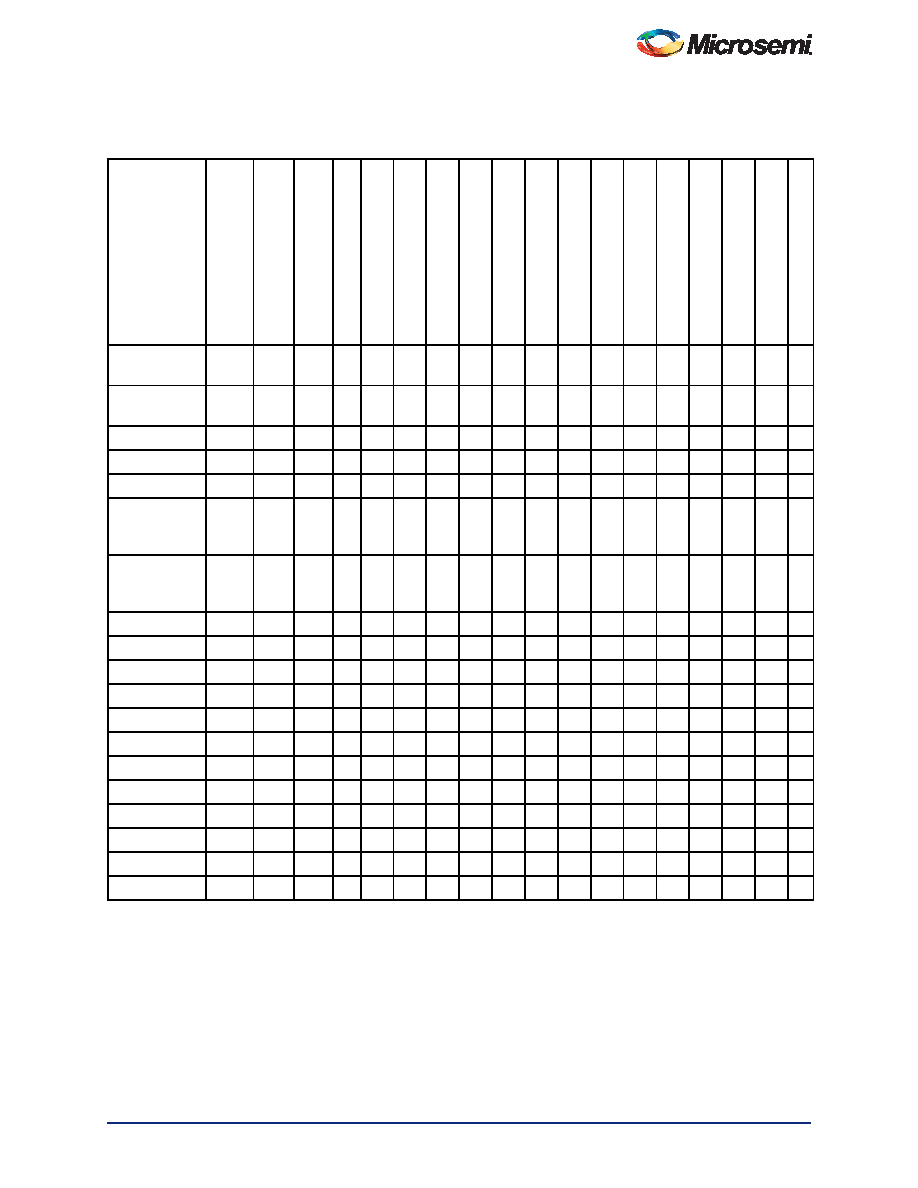
Table 2-25 Summary of I/O Timing Characteristics—Software Default Settings
Std. Speed Grade, Commercial-Case Conditions: TJ = 70°C, Worst-Case VCC = 1.425 V,
Worst-Case VCCI (per standard)
I/O Standard
D
rive
S
tre
ng
th
(mA)
Eq
ui
va
le
nt
Sof
twar
eDefau
lt
D
rive
S
tre
ng
th
Op
tio
n
1 (m
A)
Slew
Rate
C
ap
a
citive
L
o
a
d
(pF
)
Ex
tern
al
Re
sistor
(
)
t DO
U
T
(ns)
t DP
(ns)
t DI
N
(ns)
t PY
(ns)
t PYS
(ns)
t EOUT
(ns)
t ZL
(ns)
t ZH
(ns)
t LZ
(ns)
t HZ
(ns)
t ZL
S
(ns)
t ZH
S
(n
s)
Un
it
s
3.3 V LVTTL /
3.3 V LVCMOS
12
High 5
–
0.97 2.12 0.18 1.08 1.34 0.66 2.17 1.69 2.71 3.08 5.76 5.28 ns
3.3 V LVCMOS
Wide Range1, 2
100 A
12
High
5
–
0.972.960.181.421.840.662.982.283.864.366.585.87 ns
2.5 V LVCMOS
12
High
5
–
.097 2.15 0.18 1.31 1.41 0.66 2.20 1.85 2.78 2.98 5.80 5.45 ns
1.8 V LVCMOS
12
High 5
–
0.97 2.37 0.18 1.27 1.59 0.66 2.42 2.03 3.07 3.57 6.02 5.62 ns
1.5 V LVCMOS
12
High 5
–
0.97 2.69 0.18 1.47 1.77 0.66 2.75 2.30 3.24 3.67 6.35 5.89 ns
3.3 V PCI
Per
PCI
spec
–
High 10 25 3 0.97 2.38 0.18 0.96 1.42 0.66 2.43 1.80 2.72 3.08 6.03 5.39 ns
3.3 V PCI-X
Per
PCI-X
spec
–
High 10 25 3 0.97 2.38 0.19 0.92 1.34 0.66 2.43 1.80 2.72 3.08 6.03 5.39 ns
3.3 V GTL
204
–
High 10
25 0.97 1.78 0.19 2.35
–
0.66 1.80 1.78
–
5.39 5.38 ns
2.5 V GTL
204
–
High 10
25 0.97 1.85 0.19 1.98
–
0.66 1.89 1.82
–
5.49 5.42 ns
3.3 V GTL+
35
–
High 10
25 0.97 1.80 0.19 1.32
–
0.66 1.84 1.77
–
5.44 5.36 ns
2.5 V GTL+
33
–
High 10
25 0.97 1.92 0.19 1.26
–
0.66 1.96 1.80
–
5.56 5.40 ns
HSTL (I)
8
–
High 20
50 0.97 2.67 0.18 1.72
–
0.66 2.72 2.67
–
6.32 6.26 ns
HSTL (II)
15
–
High 20
25 0.97 2.55 0.18 1.72
–
0.66 2.60 2.34
–
6.20 5.93 ns
SSTL2 (I)
15
–
High 30
50 0.97 1.86 0.19 1.12
–
0.66 1.90 1.68
–
5.50 5.28 ns
SSTL2 (II)
18
–
High 30
25 0.97 1.89 0.19 1.12
–
0.66 1.93 1.62
–
5.53 5.22 ns
SSTL3 (I)
14
–
High 30
50 0.97 2.00 0.19 1.06
–
0.66 2.04 1.67
–
5.64 5.27 ns
SSTL3 (II)
21
–
High 30
25 0.97 1.81 0.19 1.06
–
0.66 1.85 1.55
–
5.45 5.14 ns
LVDS
24
–
High
–
– 0.97 1.73 0.19 1.62
––––––
––
ns
LVPECL
24
–
High
–
– 0.97 1.65 0.18 1.42
––––––
––
ns
Notes:
1. The minimum drive strength for any LVCMOS 1.2 V or LVCMOS 3.3 V software configuration when run in wide range is
±100 A. Drive strength displayed in the software is supported for normal range only. For a detailed I/V curve, refer to the
IBIS models.
2. All LVCMOS 3.3 V software macros support LVCMOS 3.3 V wide range as specified in the JESD8-B specification.
3. Resistance is used to measure I/O propagation delays as defined in PCI Specifications. See Figure 2-12 on page 2-49 for
connectivity. This resistor is not required during normal operation.
4. Output drive strength is below JEDEC specification.
5. For specific junction temperature and voltage supply levels, refer to Table 2-6 on page 2-6 for derating values.
相關(guān)PDF資料 |
PDF描述 |
|---|---|
| EPF10K50VQC240-3 | IC FLEX 10KA FPGA 50K 240-PQFP |
| EPF10K50VBC356-4N | IC FLEX 10KV FPGA 50K 356-BGA |
| EPF10K50VBC356-4 | IC FLEX 10KV FPGA 50K 356-BGA |
| A54SX16P-2TQG144I | IC FPGA SX 24K GATES 144-TQFP |
| A54SX16P-2TQ144I | IC FPGA SX 24K GATES 144-TQFP |
相關(guān)代理商/技術(shù)參數(shù) |
參數(shù)描述 |
|---|---|
| AGLE600V5-FG484 | 功能描述:IC FPGA 1KB FLASH 600K 484-FBGA RoHS:否 類別:集成電路 (IC) >> 嵌入式 - FPGA(現(xiàn)場可編程門陣列) 系列:IGLOOe 標(biāo)準(zhǔn)包裝:40 系列:SX-A LAB/CLB數(shù):6036 邏輯元件/單元數(shù):- RAM 位總計:- 輸入/輸出數(shù):360 門數(shù):108000 電源電壓:2.25 V ~ 5.25 V 安裝類型:表面貼裝 工作溫度:0°C ~ 70°C 封裝/外殼:484-BGA 供應(yīng)商設(shè)備封裝:484-FPBGA(27X27) |
| AGLE600V5-FG484I | 功能描述:IC FPGA 1KB FLASH 600K 484-FBGA RoHS:否 類別:集成電路 (IC) >> 嵌入式 - FPGA(現(xiàn)場可編程門陣列) 系列:IGLOOe 產(chǎn)品培訓(xùn)模塊:Three Reasons to Use FPGA's in Industrial Designs Cyclone IV FPGA Family Overview 特色產(chǎn)品:Cyclone? IV FPGAs 標(biāo)準(zhǔn)包裝:60 系列:CYCLONE® IV GX LAB/CLB數(shù):9360 邏輯元件/單元數(shù):149760 RAM 位總計:6635520 輸入/輸出數(shù):270 門數(shù):- 電源電壓:1.16 V ~ 1.24 V 安裝類型:表面貼裝 工作溫度:0°C ~ 85°C 封裝/外殼:484-BGA 供應(yīng)商設(shè)備封裝:484-FBGA(23x23) |
| AGLE600V5-FG896 | 制造商:ACTEL 制造商全稱:Actel Corporation 功能描述:IGLOOe Low-Power Flash FPGAs with Flash Freeze Technology |
| AGLE600V5-FG896ES | 制造商:ACTEL 制造商全稱:Actel Corporation 功能描述:IGLOOe Low-Power Flash FPGAs with Flash Freeze Technology |
| AGLE600V5-FG896I | 制造商:ACTEL 制造商全稱:Actel Corporation 功能描述:IGLOOe Low-Power Flash FPGAs with Flash Freeze Technology |
發(fā)布緊急采購,3分鐘左右您將得到回復(fù)。