- 您現(xiàn)在的位置:買賣IC網(wǎng) > PDF目錄374047 > ADV7311KST (ANALOG DEVICES INC) Multiformat 216 MHz Video Encoder with Six NSV 12-Bit DACs PDF資料下載
參數(shù)資料
| 型號(hào): | ADV7311KST |
| 廠商: | ANALOG DEVICES INC |
| 元件分類: | 顏色信號(hào)轉(zhuǎn)換 |
| 英文描述: | Multiformat 216 MHz Video Encoder with Six NSV 12-Bit DACs |
| 中文描述: | COLOR SIGNAL ENCODER, PQFP64 |
| 封裝: | PLASTIC, MS-026BCD, LQFP-64 |
| 文件頁數(shù): | 16/84頁 |
| 文件大小: | 1099K |
| 代理商: | ADV7311KST |
第1頁第2頁第3頁第4頁第5頁第6頁第7頁第8頁第9頁第10頁第11頁第12頁第13頁第14頁第15頁當(dāng)前第16頁第17頁第18頁第19頁第20頁第21頁第22頁第23頁第24頁第25頁第26頁第27頁第28頁第29頁第30頁第31頁第32頁第33頁第34頁第35頁第36頁第37頁第38頁第39頁第40頁第41頁第42頁第43頁第44頁第45頁第46頁第47頁第48頁第49頁第50頁第51頁第52頁第53頁第54頁第55頁第56頁第57頁第58頁第59頁第60頁第61頁第62頁第63頁第64頁第65頁第66頁第67頁第68頁第69頁第70頁第71頁第72頁第73頁第74頁第75頁第76頁第77頁第78頁第79頁第80頁第81頁第82頁第83頁第84頁
REV. A
–16–
ADV7310/ADV7311
MPU PORT DESCRIPTION
The ADV7310/ADV7311 support a 2-wire serial (I
2
C compat-
ible) microprocessor bus driving multiple peripherals. Two inputs,
serial data (SDA) and serial clock (SCL), carry information
between any device connected to the bus and the ADV7310/
ADV7311. Each slave device is recognized by a unique address.
The ADV7310/ADV7311 have four possible slave addresses for
both read and write operations. These are unique addresses for
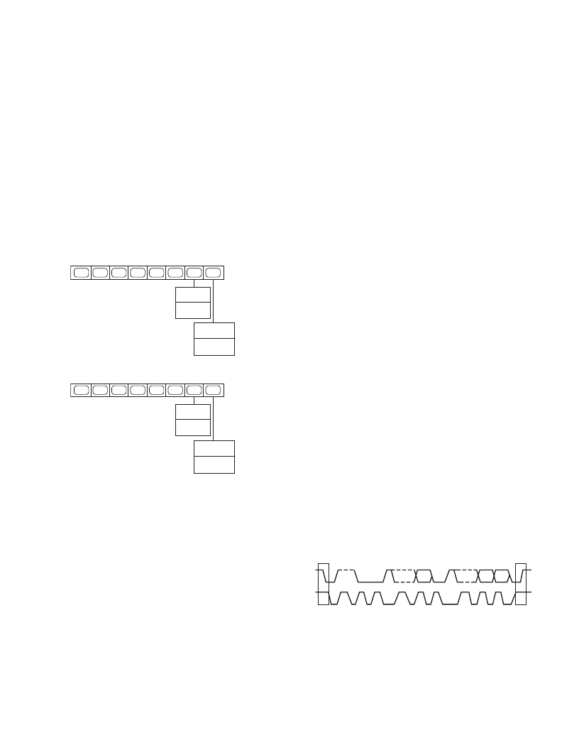
each device and are illustrated in Figure 17. The LSB sets
either a read or write operation. Logic 1 corresponds to a read
operation, while Logic 0 corresponds to a write operation. A1 is
set by setting the ALSB pin of the ADV7310/ADV7311 to
Logic 0 or Logic 1. When ALSB is set to 1, there is greater
input bandwidth on the I
2
C lines, which allows high speed data
transfers on this bus. When ALSB is set to 0, there is reduced
input bandwidth on the I
2
C lines, which means that pulses of
less than 50 ns will not pass into the I
2
C internal controller.
This mode is recommended for noisy systems.
1
1
0
1
0
1
A1
X
ADDRESS
CONTROL
SET UP BY
ALSB
READ/WRITE
CONTROL
0 WRITE
1 READ
Figure 17. ADV7310 Slave Address = D4h
0
1
0
1
0
1
A1
X
ADDRESS
CONTROL
SET UP BY
ALSB
READ/WRITE
CONTROL
0 WRITE
1 READ
Figure 18. ADV7311 Slave Address = 54h
To control the various devices on the bus, the following protocol
must be followed. First the master initiates a data transfer by
establishing a start condition, defined by a high-to-low transi-
tion on SDA while SCL remains high. This indicates that
an address/data stream will follow. All peripherals respond to
the start condition and shift the next eight bits (7-bit address +
R/W bit). The bits are transferred from MSB down to LSB. The
peripheral that recognizes the transmitted address responds by
pulling the data line low during the ninth clock pulse. This is
known as an acknowledge bit. All other devices withdraw from
the bus at this point and maintain an idle condition. The idle
condition is where the device monitors the SDA and SCL lines
waiting for the start condition and the correct transmitted address.
The R/
W
bit determines the direction of the data.
A Logic 0 on the LSB of the first byte means that the master
will write information to the peripheral. A Logic 1 on the LSB
of the first byte means that the master will read information
from the peripheral.
The ADV7310/ADV7311 acts as a standard slave device on
the bus. The data on the SDA pin is 8 bits long, supporting the
7-bit addresses plus the R/
W
bit. It interprets the first byte as
the device address and the second byte as the starting subaddress.
There is a subaddress auto-increment facility. This allows data
to be written to or read from registers in ascending subaddress
sequence starting at any valid subaddress. A data transfer is
always terminated by a stop condition. The user can also access
any unique subaddress register on a one-by-one basis without
having to update all the registers.
Stop and start conditions can be detected at any stage during the
data transfer. If these conditions are asserted out of sequence
with normal read and write operations, then they cause an
immediate jump to the idle condition. During a given SCL high
period, the user should only issue one start condition, one stop
condition, or a single stop condition followed by a single start
condition. If an invalid subaddress is issued by the user, the
ADV7310/ADV7311 will not issue an acknowledge and will return
to the idle condition. If in auto-increment mode the user exceeds
the highest subaddress, the following action will be taken:
1. In read mode, the highest subaddress register contents
will continue to be output until the master device issues
a no-acknowledge. This indicates the end of a read.
A no-acknowledge condition is when the SDA line is not
pulled low on the ninth pulse.
2. In write mode, the data for the invalid byte will not be loaded
into any subaddress register, a no-acknowledge will be issued
by the ADV7310/ADV7311, and the part will return to the
idle condition.
Before writing to the subcarrier frequency registers, it is a require-
ment that the ADV7310/ADV7311 has been reset at least once
after power-up.
The four subcarrier frequency registers must be updated, starting
with subcarrier frequency register 0 through subcarrier frequency
register 3. The subcarrier frequency will not update until the last
subcarrier frequency register byte has been received by the
ADV7310/ADV7311.
Figure 19 illustrates an example of data transfer for a write
sequence and the start and stop conditions. Figure 20 shows
bus write and read sequences.
SDATA
SCLOCK
START ADRR R/
W
ACK
SUBADDRESS ACK
DATA
ACK
STOP
1–7
8
9
S
1–7
8
9
1–7
8
9
P
Figure 19. Bus Data Transfer
相關(guān)PDF資料 |
PDF描述 |
|---|---|
| ADV7312 | Multiformat 11-Bit HDTV Video Encoder |
| ADV7312KST | Multiformat 11-Bit HDTV Video Encoder |
| ADV7320KSTZ | Multiformat 216 MHz Video Encoder with Six NSV 12-Bit DACs |
| ADV7320 | Multiformat 216 MHz Video Encoder with Six NSV 12-Bit DACs |
| ADV7321 | Multiformat 216 MHz Video Encoder with Six NSV 12-Bit DACs |
相關(guān)代理商/技術(shù)參數(shù) |
參數(shù)描述 |
|---|---|
| ADV7311KST | 制造商:Analog Devices 功能描述:Video IC |
| ADV7312 | 制造商:AD 制造商全稱:Analog Devices 功能描述:Multiformat 11-Bit HDTV Video Encoder |
| ADV7312KST | 制造商:AD 制造商全稱:Analog Devices 功能描述:Multiformat 11-Bit HDTV Video Encoder |
| ADV7314 | 制造商:AD 制造商全稱:Analog Devices 功能描述:Multiformat 216 MHz Video Encoder with Six NSV 14-Bit DACs |
| ADV7314KST | 制造商:AD 制造商全稱:Analog Devices 功能描述:Multiformat 216 MHz Video Encoder with Six NSV 14-Bit DACs |
發(fā)布緊急采購,3分鐘左右您將得到回復(fù)。