- 您現(xiàn)在的位置:買賣IC網(wǎng) > PDF目錄375269 > ADV7195KST (ANALOG DEVICES INC) Multiformat Progressive Scan/HDTV Encoder with Three 11-Bit DACs and 10-Bit Data Input PDF資料下載
參數(shù)資料
| 型號(hào): | ADV7195KST |
| 廠商: | ANALOG DEVICES INC |
| 元件分類: | 消費(fèi)家電 |
| 英文描述: | Multiformat Progressive Scan/HDTV Encoder with Three 11-Bit DACs and 10-Bit Data Input |
| 中文描述: | SPECIALTY CONSUMER CIRCUIT, PQFP52 |
| 封裝: | PLASTIC, MQFP-52 |
| 文件頁數(shù): | 30/36頁 |
| 文件大小: | 499K |
| 代理商: | ADV7195KST |
第1頁第2頁第3頁第4頁第5頁第6頁第7頁第8頁第9頁第10頁第11頁第12頁第13頁第14頁第15頁第16頁第17頁第18頁第19頁第20頁第21頁第22頁第23頁第24頁第25頁第26頁第27頁第28頁第29頁當(dāng)前第30頁第31頁第32頁第33頁第34頁第35頁第36頁
REV. 0
ADV7195
–30–
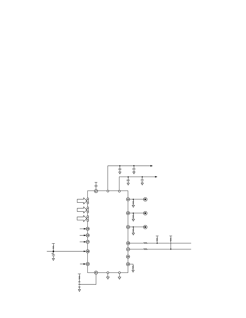
PC BOARD LAYOUT CONSIDERATIONS
The ADV7195 is optimally designed for lowest noise perfor-
mance, both radiated and conducted noise. To complement the
excellent noise performance of the ADV7195, it is imperative
that great care be given to the PC board layout.
The layout should be optimized for lowest noise on the ADV7195
power and ground lines. This can be achieved by shielding the
digital inputs and providing good decoupling. The lead length
between groups of V
AA
and AGND, and V
DD
and DGND pins,
should be kept as short as possible to minimize inductive ringing.
It is recommended that a four-layer printed circuit board be
used. With power and ground planes separating the layer of the
signal carrying traces of the components and solder-side layer.
Placement of components should be considered to separate
noisy circuits such as crystal clocks, high-speed logic circuitry,
and analog circuitry.
There should be a separate analog ground plane (AGND) and
a separate digital ground plane (GND).
Power planes should encompass a digital power plane (V
DD
)
and an analog power plane (V
AA
). The analog power plane
should contain the DACs and all associated circuitry, and the
V
REF
circuitry.
The digital power plane should contain all logic circuitry. The
analog and digital power planes should be individually con-
nected to the common power plane at one single point through
a suitable filtering device such as a ferrite bead.
300
5k
5k
MPU BUS
4.7k
V
AA
POWER SUPPLY DECOUPLING
FOR EACH POWER SUPPLY GROUP
ALSB
DV
RESET
CLKIN
R
SET
SDA
SCL
DAC A
V
DD
VSYNC
/TSYNC
ADV7195
UNUSED
INPUTS
SHOULD BE
GROUNDED
DAC B
100
HSYNC
/
SYNC
DAC C
27MHz, 74.25MHz OR
74.1758MHz CLOCK
4.7k
4.7 F
6.3V
300
300
100
2.47k OR
2.82k
10nF
0.1 F
Y OUTPUT
Pr (V) OUTPUT
Pb (U) OUTPUT
V
REF
GND
13, 52
AGND
26, 33
Y0
–
Y9
Cr0
–
Cr9
Cb/Cr0
–
Cb/Cr9
0.1 F
10nF
0.1 F
24, 35
1, 12
V
AA
V
AA
COMP
V
AA
V
AA
V
AA
V
AA
V
AA
Figure 57. Circuit Layout
DAC TERMINATION AND LAYOUT CONSIDERATIONS
Voltage Reference
The ADV7195 contains an onboard voltage reference. The V
REF
pin is normally terminated to V
AA
through a 0.1
μ
F capacitor when
the internal V
REF
is used. Alternatively, the ADV7195 can be
used with an external V
REF
(AD589).
Resistor R
SET
is connected between the R
SET
pin and AGND
and is used to control the full-scale output current and there-
fore the DAC voltage output levels. For full-scale output, R
SET
must have a value of 2470
; R
LOAD
has a value of 300
.
When an input range of 0–1023 is selected, the value of R
SET
must be 2820
.
The ADV7195 has three analog outputs, corresponding to Y,
Pr, Pb video signals. The DACs must be used with external
buffer circuits in order to provide sufficient current to drive an
output device. Suitable op amps are the AD8009, AD8002,
AD8001, or AD8057. To calculate the output full-scale current
and voltage, the following equations should be used:
V
OUT
=
I
OUT
×
R
LOAD
I
OUT
= [
V
REF
×
k
]/
R
SET
k
= 5.66,
for I/P Ranges
64–940, 64–960,
O/P Standards
EIA-
770.1–3
k=
6.46
, F
CI
Input Ranges
0–1023
, Output Standard
RS-
170/343
A
V
REF
=
1.235
V
相關(guān)PDF資料 |
PDF描述 |
|---|---|
| ADV7196 | Multiformat Progressive Scan/HDTV Encoder with Three 11-Bit DACs, 10-Bit Data Input, and Macrovision |
| ADV7196A | Multiformat Progressive Scan/HDTV Encoder with Three 11-Bit DACs, 10-Bit Data Input, and Macrovision |
| ADV7196AKS | Multiformat Progressive Scan/HDTV Encoder with Three 11-Bit DACs, 10-Bit Data Input, and Macrovision |
| ADV7197 | Multiformat HDTV Encoder with Three 11-Bit DACs |
| ADV7197KST | Multiformat HDTV Encoder with Three 11-Bit DACs |
相關(guān)代理商/技術(shù)參數(shù) |
參數(shù)描述 |
|---|---|
| ADV7195KSZ | 制造商:Analog Devices 功能描述:Video Encoder 3DAC 11-Bit 52-Pin MQFP |
| ADV7196 | 制造商:AD 制造商全稱:Analog Devices 功能描述:Multiformat Progressive Scan/HDTV Encoder with Three 11-Bit DACs, 10-Bit Data Input, and Macrovision |
| ADV7196A | 制造商:AD 制造商全稱:Analog Devices 功能描述:Multiformat Progressive Scan/HDTV Encoder with Three 11-Bit DACs, 10-Bit Data Input, and Macrovision |
| ADV7196AKS | 制造商:AD 制造商全稱:Analog Devices 功能描述:Multiformat Progressive Scan/HDTV Encoder with Three 11-Bit DACs, 10-Bit Data Input, and Macrovision |
| ADV7197 | 制造商:AD 制造商全稱:Analog Devices 功能描述:Multiformat HDTV Encoder with Three 11-Bit DACs |
發(fā)布緊急采購,3分鐘左右您將得到回復(fù)。