- 您現在的位置:買賣IC網 > PDF目錄374039 > ADUC841 (Analog Devices, Inc.) MicroConverter 12-Bit ADCs and DACs with Embedded High Speed 62-kB Flash MCU PDF資料下載
參數資料
| 型號: | ADUC841 |
| 廠商: | Analog Devices, Inc. |
| 英文描述: | MicroConverter 12-Bit ADCs and DACs with Embedded High Speed 62-kB Flash MCU |
| 中文描述: | MicroConverter的12位ADC和嵌入式高速DAC的62 - kB的閃存微控制器 |
| 文件頁數: | 59/88頁 |
| 文件大小: | 903K |
| 代理商: | ADUC841 |
第1頁第2頁第3頁第4頁第5頁第6頁第7頁第8頁第9頁第10頁第11頁第12頁第13頁第14頁第15頁第16頁第17頁第18頁第19頁第20頁第21頁第22頁第23頁第24頁第25頁第26頁第27頁第28頁第29頁第30頁第31頁第32頁第33頁第34頁第35頁第36頁第37頁第38頁第39頁第40頁第41頁第42頁第43頁第44頁第45頁第46頁第47頁第48頁第49頁第50頁第51頁第52頁第53頁第54頁第55頁第56頁第57頁第58頁當前第59頁第60頁第61頁第62頁第63頁第64頁第65頁第66頁第67頁第68頁第69頁第70頁第71頁第72頁第73頁第74頁第75頁第76頁第77頁第78頁第79頁第80頁第81頁第82頁第83頁第84頁第85頁第86頁第87頁第88頁
ADuC841/ADuC842/ADuC843
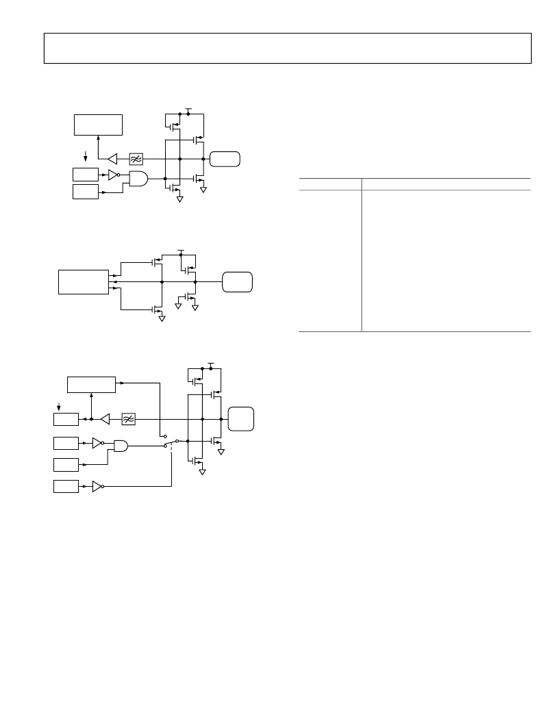
MOSI is shared with P3.3 and, as such, has the same
configuration as the one shown in Figure 61.
Rev. 0 | Page 59 of 88
MCO
I2CM
Q3
Q4
SCLOCK
PIN
Q2
Q1
(OFF)
DV
DD
50ns GLITCH
REJECTION FILTER
SPE = 0 (I
2
C ENABLE)
HARDWARE I
2
C
(SLAVE ONLY)
SFR
BITS
0
Figure 63. SCLOCK Pin I/O Functional Equivalent in I
2
C Mode
Q3
Q1
Q2 (OFF)
DV
DD
Q4 (OFF)
SDATA/
MOSI
PIN
SPE = 1 (SPI ENABLE)
HARDWARE SPI
(MASTER/SLAVE)
0
Figure 64. SDATA/MOSI Pin I/O Functional Equivalent in SPI Mode
Q3
Q4
Q2
Q1
(OFF)
DV
DD
MCO
SDATA/
MOSI
PIN
50ns GLITCH
REJECTION FILTER
SPE = 0 (I
2
C ENABLE)
HARDWARE I
2
C
(SLAVE ONLY)
SFR
BITS
MCI
MDE
I2CM
0
Figure 65. SDATA/MOSI Pin I/O Functional Equivalent in I
2
C Mode
Read-Modify-Write Instructions
Some 8051 instructions that read a port read the latch while
others read the pin. The instructions that read the latch rather
than the pins are the ones that read a value, possibly change it,
and then rewrite it to the latch. These are called read-modify-
write instructions, which are listed below. When the destination
operand is a port or a port bit, these instructions read the latch
rather than the pin.
Table 27. Read-Write-Modify Instructions
Instruction
Description
ANL
Logical AND, e.g., ANL P1, A
ORL
(Logical OR, e.g., ORL P2, A
XRL
(Logical EX-OR, e.g., XRL P3, A
JBC
Jump if Bit = 1 and clear bit, e.g., JBC P1.1,
LABEL
CPL
Complement bit, e.g., CPL P3.0
INC
Increment, e.g., INC P2
DEC
Decrement, e.g., DEC P2
DJNZ
Decrement and Jump if Not Zero, e.g., DJNZ
P3, LABEL
MOV PX.Y, C
1
Move Carry to Bit Y of Port X
CLR PX.Y
1
Clear Bit Y of Port X
SETB PX.Y
1
Set Bit Y of Port X
1
These instructions read the port byte (all 8 bits), modify the addressed bit,
and then write the new byte back to the latch.
Read-modify-write instructions are directed to the latch rather
than to the pin to avoid a possible misinterpretation of the
voltage level of a pin. For example, a port pin might be used to
drive the base of a transistor. When 1 is written to the bit, the
transistor is turned on. If the CPU then reads the same port bit
at the pin rather than the latch, it reads the base voltage of the
transistor and interprets it as a Logic 0. Reading the latch rather
than the pin returns the correct value of 1.
相關PDF資料 |
PDF描述 |
|---|---|
| ADUC841BCP62-3 | MicroConverter 12-Bit ADCs and DACs with Embedded High Speed 62-kB Flash MCU |
| ADUC841BCP62-5 | Cable Gland (Clamp); Connector Shell Size:10SL, 12S; Thread Size:5/8-24; Approval Categories:MIL-C-5015; Series:97 RoHS Compliant: Yes |
| ADUC841BCP8-3 | 10-823955-004 |
| ADUC841BCP8-5 | Cable Gland (Clamp); Connector Shell Size:14, 14S; Thread Size:3/4-20; Body Material:Zinc Alloy |
| ADUC841BS62-3 | MicroConverter 12-Bit ADCs and DACs with Embedded High Speed 62-kB Flash MCU |
相關代理商/技術參數 |
參數描述 |
|---|---|
| ADUC841BCP32-5 | 制造商:Analog Devices 功能描述:MICROCONVERTER 1-CYCLE VERSION ADUC829 - Trays |
| ADUC841BCP62-3 | 制造商:Analog Devices 功能描述:MCU 8-Bit ADuC8xx 8052 CISC 62KB Flash 3V 56-Pin LFCSP EP 制造商:Rochester Electronics LLC 功能描述:8BIT CISC 62KB FLASH 20MHZ 3.3V 56LFCSP - Bulk |
| ADUC841BCP62-5 | 制造商:Analog Devices 功能描述:MCU 8-Bit ADuC8xx 8052 CISC 62KB Flash 5V 56-Pin LFCSP EP |
| ADUC841BCP8-3 | 制造商:Analog Devices 功能描述:MCU 8-bit ADuC8xx 8052 CISC 62KB Flash 3V 56-Pin LFCSP EP 制造商:Rochester Electronics LLC 功能描述:8BIT CISC 62KB FLASH 20MHZ 3.3V 56LFCSP - Bulk |
| ADUC841BCP8-5 | 制造商:AD 制造商全稱:Analog Devices 功能描述:MicroConverter 12-Bit ADCs and DACs with Embedded High Speed 62-kB Flash MCU |
發(fā)布緊急采購,3分鐘左右您將得到回復。